


 产品分类
产品分类
基于Xilinx公司的Zybo Zynq-7000ARM-FPGA全编程SoC解决方案
 406
406
 拍明
拍明
原标题:Xilinx Zybo Zynq-7000ARM-FPGA全编程SoC解决方案
Xilinx公司的Zynq®-7000系列是基于Xilinx全编程的系统级芯片(SoC)架构,集成了功能丰富的双核或单核ARM® Cortex™-A9处理系统(PS)和28nm Xilinx可编程逻辑.ARM® Cortex™-A9 CPU是处理系统的心脏,包括了片上存储器,外接存储器接口和各种外设连接接口.主要用在汽车辅助驾驭,驾驭信息和娱乐系统,广播照相机,工业马达控制,工业网络和机器视角,IP和智能照相机,LTE无线和基带,医疗诊断和成像,多功能打印机以及视频和夜视设备.本文介绍了Zynq-7000 FPGA主要特性和架构图,以及Zybo Zynq-7000 ARM/FPGA SoC培训板主要特性和优势,主要元件分布图与电路图.
The Zynq®-7000 family is based on the Xilinx All Programmable SoC architecture. These products integrate a feature-rich dual-core or single-core ARM® Cortex™-A9 based processing system (PS) and 28 nm Xilinx programmable logic (PL) in a single device. The ARM Cortex-A9 CPUs are the heart of the PS and also include on-chip memory, external memory interfaces, and a rich set of peripheral connectivity interfaces.
The Zynq-7000 family offers the flexibility and scalability of an FPGA, while providing performance, power, and ease of usetypically associated with ASIC and ASSPs. The range of devices in the Zynq-7000 family allows designers to targetcost-sensitive as well as high-performance applications from a single platform using industry-standard tools. While eachdevice in the Zynq-7000 family contains the same PS, the PL and I/O resources vary between the devices. As a result, theZynq-7000 and Zynq-7000S SoCs are able to serve a wide range of applications including:
• Automotive driver assistance, driver information, and infotainment
• Broadcast camera
• Industrial motor control, industrial networking, and machine vision
• IP and Smart camera
• LTE radio and baseband
• Medical diagnostics and imaging
• Multifunction printers
• Video and night vision equipment
The Zynq-7000 architecture enables implementation of custom logic in the PL and custom software in the PS. It allows forthe realization of unique and differentiated system functions. The integration of the PS with the PL allows levels ofperformance that two-chip solutions (e.g., an ASSP with an FPGA) cannot match due to their limited I/O bandwidth, latency,and power budgets.
Xilinx offers a large number of soft IP for the Zynq-7000 family. Stand-alone and Linux device drivers are available for theperipherals in the PS and the PL. The Vivado® Design Suite development environment enables a rapid productdevelopment for software, hardware, and systems engineers. Adoption of the ARM-based PS also brings a broad range ofthird-party tools and IP providers in combination with Xilinx’s existing PL ecosystem.
The inclusion of an application processor enables high-level operating system support, e.g., Linux. Other standard operatingsystems used with the Cortex-A9 processor are also available for the Zynq-7000 family.
The PS and the PL are on separate power domains, enabling the user of these devices to power down the PL for powermanagement if required. The processors in the PS always boot first, allowing a software centric approach for PLconfiguration. PL configuration is managed by software running on the CPU, so it boots similar to an ASSP.
Zynq-7000 FPGA主要特性:
Processing System (PS)
ARM Cortex-A9 Based
Application Processor Unit (APU)
• 2.5 DMIPS/MHz per CPU
• CPU frequency: Up to 1 GHz
• Coherent multiprocessor support
• ARMv7-A architecture
• TrustZone® security
• Thumb®-2 instruction set
• Jazelle® RCT execution Environment Architecture
• NEON™ media-processing engine
• Single and double precision Vector Floating Point Unit (VFPU)
• CoreSight™ and Program Trace Macrocell (PTM)
• Timer and Interrupts
• Three watchdog timers
• One global timer
• Two triple-timer counters
Caches
• 32 KB Level 1 4-way set-associative instruction and data caches(independent for each CPU)
• 512 KB 8-way set-associative Level 2 cache(shared between the CPUs)
• Byte-parity support
On-Chip Memory
• On-chip boot ROM
• 256 KB on-chip RAM (OCM)
• Byte-parity support
External Memory Interfaces
• Multiprotocol dynamic memory controller
• 16-bit or 32-bit interfaces to DDR3, DDR3L, DDR2, or LPDDR2memories
• ECC support in 16-bit mode
• 1GB of address space using single rank of 8-, 16-, or 32-bit-widememories
• Static memory interfaces
• 8-bit SRAM data bus with up to 64 MB support
• Parallel NOR flash support
• ONFI1.0 NAND flash support (1-bit ECC)
• 1-bit SPI, 2-bit SPI, 4-bit SPI (quad-SPI), or two quad-SPI (8-bit)serial NOR flash
8-Channel DMA Controller
• Memory-to-memory, memory-to-peripheral, peripheral-to-memory,and scatter-gather transaction support
I/O Peripherals and Interfaces
• Two 10/100/1000 tri-speed Ethernet MAC peripherals withIEEE Std 802.3 and IEEE Std 1588 revision 2.0 support
• Scatter-gather DMA capability
• Recognition of 1588 rev. 2 PTP frames
• GMII, RGMII, and SGMII interfaces
• Two USB 2.0 OTG peripherals, each supporting up to 12 Endpoints
• USB 2.0 compliant device IP core
• Supports on-the-go, high-speed, full-speed, and low-speedmodes
• Intel EHCI compliant USB host
• 8-bit ULPI external PHY interface
• Two full CAN 2.0B compliant CAN bus interfaces
• CAN 2.0-A and CAN 2.0-B and ISO 118981-1 standardcompliant
• External PHY interface
• Two SD/SDIO 2.0/MMC3.31 compliant controllers
• Two full-duplex SPI ports with three peripheral chip selects
• Two high-speed UARTs (up to 1 Mb/s)
• Two master and slave I2C interfaces
• GPIO with four 32-bit banks, of which up to 54 bits can be used withthe PS I/O (one bank of 32b and one bank of 22b) and up to 64 bits(up to two banks of 32b) connected to the Programmable Logic
• Up to 54 flexible multiplexed I/O (MIO) for peripheral pin assignments
Interconnect
• High-bandwidth connectivity within PS and between PS and PL
• ARM AMBA® AXI based
• QoS support on critical masters for latency and bandwidth control
Programmable Logic (PL)
Configurable Logic Blocks (CLB)
• Look-up tables (LUT)
• Flip-flops
• Cascadeable adders
36 Kb Block RAM
• True Dual-Port
• Up to 72 bits wide
• Configurable as dual 18 Kb block RAM
DSP Blocks
• 18 x 25 signed multiply
• 48-bit adder/accumulator
• 25-bit pre-adder
Programmable I/O Blocks
• Supports LVCMOS, LVDS, and SSTL
• 1.2V to 3.3V I/O
• Programmable I/O delay and SerDes
JTAG Boundary-Scan
• IEEE Std 1149.1 Compatible Test Interface
PCI Express® Block
• Supports Root complex and End Point configurations
• Supports up to Gen2 speeds
• Supports up to 8 lanes
Serial Transceivers
• Up to 16 receivers and transmitters
• Supports up to 12.5 Gb/s data rates
Two 12-Bit Analog-to-Digital Converters
• On-chip voltage and temperature sensing
• Up to 17 external differential input channels
• One million samples per second maximum conversion rate
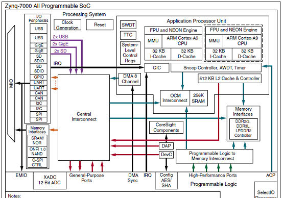
图1.Zynq-7000 FPGA架构图
Zybo Zynq-7000 ARM/FPGA SoC培训板
The Zybo (Zynq™ Board) is a feature-rich, ready-to-use, entry-level embedded software and digital circuit development platform built around the smallest member of the Xilinx Zynq-7000 family, the Z-7010. The Z-7010 is based on the Xilinx® All Programmable System-on-Chip (AP SoC) architecture, which tightly integrates a dual-core ARM Cortex-A9 processor with Xilinx 7-series field programmable gate array (FPGA) logic. When coupled with the rich set of multimedia and connectivity peripherals available on the Zybo, the Zynq Z-7010 can host a whole system design. The on-board memories, video and audio I/O, dual-role USB, Ethernet and SD slot will have your design up-and-ready with no additional hardware needed. Additionally, six Pmod connectors are available to put any design on an easy growth path. The Zybo provides an ultra-low cost alternative to the ZedBoard for designers that don’t require the high-density I/O of the FMC connector, but still wish to leverage the massive processing power and extensibility of the Zynq AP SoC architecture.
Zybo Zynq-7000 ARM/FPGA SoC培训板主要特性和优势:
128 Mb Serial Flash w/ QSPI interface
16-bits per pixel VGA output port
240 KB Block RAM
28,000 logic cells
512 MB x32 DDR3 w/ 1050Mbps bandwidth
650 MHz dual-core Cortex™-A9 processor
80 DSP slices
Audio codec with headphone out, microphone and line in jacks
DDR3 memory controller with 8 DMA channels
Dual-role (Source/Sink) HDMI port
External EEPROM (programmed with 48-bit globally unique EUI-48/64™ compatible identifier)
GPIO: 6 pushbuttons, 4 slide switches, 5 LEDs
High-bandwith peripheral controllers: 1G Ethernet, USB 2.0, SDIO
Low-bandwidth peripheral controller: SPI, UART, I2C
OTG USB 2.0 PHY (supports host and device)
On-board JTAG programming and UART to USB converter
On-chip dual channel, 12-bit, 1 MSPS analog-to-digital converter (XADC)
Six Pmod ports (1 processor-dedicated, 1 dual analog/digital)
Trimode (1Gbit/100Mbit/10Mbit) Ethernet PHY
Xilinx Zynq-7000 (XC7Z010-1CLG400C)
microSD slot (supports Linux file system)
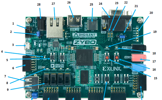
图2.Zybo Zynq-7000 ARM/FPGA SoC培训板外形图
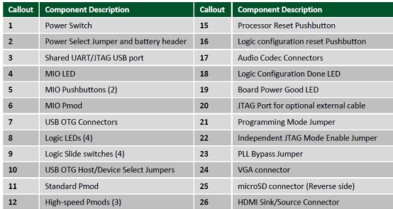
Zybo Zynq-7000 ARM/FPGA SoC培训板数字元件对应表:
详情请见:
责任编辑:HanFeng
【免责声明】
1、本文内容、数据、图表等来源于网络引用或其他公开资料,版权归属原作者、原发表出处。若版权所有方对本文的引用持有异议,请联系拍明芯城(marketing@iczoom.com),本方将及时处理。
2、本文的引用仅供读者交流学习使用,不涉及商业目的。
3、本文内容仅代表作者观点,拍明芯城不对内容的准确性、可靠性或完整性提供明示或暗示的保证。读者阅读本文后做出的决定或行为,是基于自主意愿和独立判断做出的,请读者明确相关结果。
4、如需转载本方拥有版权的文章,请联系拍明芯城(marketing@iczoom.com)注明“转载原因”。未经允许私自转载拍明芯城将保留追究其法律责任的权利。
拍明芯城拥有对此声明的最终解释权。
相关资讯
:
基于MC33771主控芯片的新能源锂电池管理系统解决方案

AMIC110 32位Sitara ARM MCU开发方案

基于AMIC110多协议可编程工业通信处理器的32位Sitara ARM MCU开发方案

基于展讯SC9820超低成本LTE芯片平台的儿童智能手表解决方案

基于TI公司的AM437x双照相机参考设计

基于MTK6580芯片的W2智能手表解决方案


 2012- 2022 拍明芯城ICZOOM.com 版权所有 客服热线:400-693-8369 (9:00-18:00)


