基于ADI公司的AD4003 18位2 MSPS精密SAR ADC评估方案
 257
257
 拍明
拍明
原标题:ADI AD4003 18位2 MSPS精密SAR ADC评估方案
ADI公司的AD4003是低噪声低功耗高速18位,2 MSPS精密逐次逼近型寄存器(SAR)模数转换器(ADC). 采用1.8 V电源供电,具有±VREF全差分输入范围,VREF范围为2.4 V至5.1 V, INL为±1.0 LSB(±3.8 ppm,最大值),保证18位无丢失码,主要用在自动测试设备
机器自动化,医疗设备,电池供电设备和精密数据采集系统.本文介绍了AD4003主要特性,功能框图和几种应用电路,以及AD4000/AD4003评估板主要特性,框图,电路图,材料清单和PCB设计图.
The AD4003 is a low noise, low power, high speed, 18-bit, 2 MSPSprecision successive approximation register (SAR) analog-to-digitalconverter (ADC). It incorporates ease of use features thatlower the signal chain power, reduce signal chain complexity, andenable higher channel density. The high-Z mode, coupled with along acquisition phase, eliminates the need for a dedicated highpower, high speed ADC driver, thus broadening the range of lowpower precision amplifiers that can drive this ADC directly, whilestill achieving optimum performance. The input span compressionfeature enables the ADC driver amplifier and the ADC to operateoff common supply rails without the need for a negative supplywhile preserving the full ADC code range. The low serialperipheral interface (SPI) clock rate requirement reduces thedigital input/output power consumption, broadens processoroptions, and simplifies the task of sending data across digitalisolation.
Operating from a 1.8 V supply, the AD4003 has a ±VREF fully differentialinput range with VREF ranging from 2.4 V to 5.1 V. The AD4003consumes only 16 mW at 2 MSPS with a minimum of 75 MHzSCK rate in turbo mode and achieves ±1.0 LSB (±3.8 ppm) INLmaximum, guaranteed no missing codes at 18 bits with 100.5 dBtypical SNR. The reference voltage is applied externally and canbe set independently of the supply voltage.
The SPI-compatible versatile serial interface features seven differentmodes including the ability, using the SDI input, to daisy-chainseveral ADCs on a single 3-wire bus and provides an optional busyindicator. The AD4003 is compatible with 1.8 V, 2.5 V, 3 V, and
5 V logic, using the separate VIO supply.
The AD4003 is available in a 10-lead MSOP or a 10-lead LFCSPwith operation specified from −40°C to +125°C. The device ispin compatible with the 16-bit, 2 MSPS AD4000.
AD4003主要特性:
Throughput: 2 MSPS maximum
INL: ±1.0 LSB (±3.8 ppm) maximum
Guaranteed 18-bit no missing codes
Low power
9.5 mW at 2 MSPS (VDD only)
80 μW at 10 kSPS, 16 mW at 2 MSPS (total)
SNR: 100.5 dB typical at 1 kHz, 99 dB typical at 100 kHz
THD: −123 dB typical at 1 kHz, −100 dB typical at 100 kHz
Ease of use features reduce system power and complexity
Input overvoltage clamp circuit
Reduced nonlinear input charge kickback
High-Z mode
Long acquisition phase
Input span compression
Fast conversion time allows low SPI clock rates
SPI-programmable modes, read/write capability, status word
Differential analog input range: ±VREF
0 V to VREF with VREF between 2.4 V to 5.1 V
Single 1.8 V supply operation with 1.71 V to 5.5 V logic interface
SAR architecture: no latency/pipeline delay
Guaranteed operation: −40°C to 125°C
Serial interface SPI-/QSPI-/MICROWIRE-/DSP-compatible
Ability to daisy-chain multiple ADCs and busy indicator
10-lead package: 3 mm × 3 mm LFCSP and 3 mm × 4.90 mmMSOP
AD4003应用:
Automatic test equipment
Machine automation
Medical equipment
Battery-powered equipment
Precision data acquisition systems

图1.AD4003功能框图

图2.AD4003多个电源的应用电路图

图3.AD4003单电源的应用电路图

图4.AD4003全差分放大器的应用电路图

图4.AD4003带全差分放大器的单端-差分转换应用电路图
AD4000/AD4003评估板
The AD4000/AD4003 family evaluation board covers the ease of use 16-/18-bit precision SAR ADCs. The AD4000/AD4003 are a low power 16-bit/18-bit precision SAR ADCs that offer very high performance with throughputs up to 2 MSPS. The evaluation board is designed to demonstrate the performance of the AD4000/ AD4003 family of ADCs and to provide an easy to understand interface for a variety of system applications. A full description of these products is available in their respective data sheets, which should be consulted when using this evaluation board.
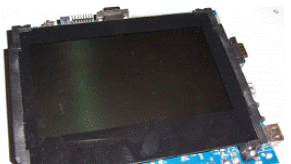
The EVAL-AD4000FMZ/EVAL-AD4003FMCZ evaluation boards (see Figure 1) are ideal for use with Analog Devices, Inc., high speed system demonstration platform (EVAL-SDP-CH1Z). These evaluation boards interface to the SDP-H1 board via a 120-pin connector. SMA connectors, JP2 and JP3, are provided for the low noise analog signal source.
On-board components include a high precision buffered band gap 5.0 V reference (the ADR4550), a reference buffer (the ADA4807-1), a common-mode buffer (the ADA4807-1), a signal conditioning circuit with two op amps (the ADA4807-1), and a power supply to derive the necessary voltage levels to supply all voltage needs.
AD4000/AD4003评估板主要特性:
Fully featured evaluation board for 10-lead precision ADCs
Versatile analog signal conditioning circuitry
On-board reference, reference buffers, and ADC drivers
PC software for control and data analysis of time and frequency domain
System demonstration platform compatible (EVAL-SDP-CH1Z)
AD4000/AD4003评估板包括:
AD4000/AD4003 evaluation board
12 V wall adapter power supply

图5.AD400x评估板外形图

图6.AD400x评估板框图
AD400x评估板材料清单:


详情请见:
责任编辑:HanFeng
【免责声明】
1、本文内容、数据、图表等来源于网络引用或其他公开资料,版权归属原作者、原发表出处。若版权所有方对本文的引用持有异议,请联系拍明芯城(marketing@iczoom.com),本方将及时处理。
2、本文的引用仅供读者交流学习使用,不涉及商业目的。
3、本文内容仅代表作者观点,拍明芯城不对内容的准确性、可靠性或完整性提供明示或暗示的保证。读者阅读本文后做出的决定或行为,是基于自主意愿和独立判断做出的,请读者明确相关结果。
4、如需转载本方拥有版权的文章,请联系拍明芯城(marketing@iczoom.com)注明“转载原因”。未经允许私自转载拍明芯城将保留追究其法律责任的权利。
拍明芯城拥有对此声明的最终解释权。


 产品分类
产品分类




 2012- 2022 拍明芯城ICZOOM.com 版权所有 客服热线:400-693-8369 (9:00-18:00)


