


 产品分类
产品分类
基于Maxim的MAX16833高压高亮(HB) LED驱动方案
 282
282
 拍明
拍明
原标题:Maxim MAX16833高压高亮(HB) LED驱动方案
Maxim公司的MAX16833/B/C/D/G是峰值电流控制的LED驱动器,适用于升压,降压-升压,SEPIC,反激和高边降压拓扑.输入电压5V-65V,最大输出电压65V,集成了高边pMOS调光MOSFET驱动器和高边电流检测放大器,可编工作频率100kHz 到1MHz,具有短路,过压和热关断保护以及故障指示输出,工作温度-40°C到+125°C,主要用在汽车外部照明装置,商业,工业和建筑物照明.本文介绍了MAX16833优势和特性,功能框图,以及评估板MAX16833 EVK主要特性,电路图,材料清单和PCB设计图.
The MAX16833, MAX16833B, MAX16833C, MAX16833D, and MAX16833G are peak current-mode-controlled LED drivers for boost, buck-boost, SEPIC, flyback, and high-side buck topologies. A dimming driver designed to drive an external p-channel in series with the LED string pro vides wide-range dimming control. This feature provides extremely fast PWM current switching to the LEDs with no transient overvoltage or undervoltage conditions. In addition to PWM dimming, the ICs provide analog dimming using a DC input at ICTRL. The ICs sense the LED current at the high side of the LED string.
A single resistor from RT/SYNC to ground sets the switching frequency from 100kHz to 1MHz, while an external clock signal capacitively coupled to RT/SYNC allows the ICs to synchronize to an external clock. In the MAX16833/C/G, the switching frequency can be dithered for spread-spectrum applications. The MAX16833B/D instead provide a 1.64V reference voltage with a 2% tolerance.
The ICs operate over a wide 5V to 65V supply range and include a 3A sink/source gate driver for driving a power MOSFET in high-power LED driver applications. Additional features include a fault-indicator output (FLT) for short or overtemperature conditions and an overvolt age-protection sense input (OVP) for overvoltage protec tion. High-side current sensing combined with a p-channel dimming MOSFET allow the positive terminal of the LED string to be shorted to the positive input terminal or to the negative input terminal without any damage. This is a unique feature of the ICs.
MAX16833优势和特性:
Integration Minimizes BOM for High-Brightness LED Driver with a Wide Input Range Saving Space and Cost+5V to +65V Wide Input Voltage Range with a Maximum 65V Boost Output
Integrated High-Side pMOS Dimming MOSFET Driver (Allows Single-Wire Connection to LEDs)
ICTRL Pin for Analog Dimming
Integrated High-Side Current-Sense Amplifier
Full-Scale, High-Side, Current-Sense Voltage of200mV
Simple to Optimize for Efficiency, Board Space, and Input Operating RangeBoost, SEPIC, and Buck-Boost Single-Channel LED Drivers
2% Accurate 1.64V Reference (MAX16833B/D)
Programmable Operating Frequency (100kHz to1MHz) with Synchronization Capability
Frequency Dithering for Spread-Spectrum Applications (MAX16833/C/G)
Thermally Enhanced 5mm x 4.4mm, 16-PinTSSOP Package with Exposed Pad
Protection Features and Wide Temperature Range Increase System Reliability Short-Circuit, Overvoltage, and Thermal Protection
Fault-Indicator Output
-40°C to +125°C Operating Temperature Range
MAX16833应用:
Automotive Exterior Lighting: High-Beam/Low-Beam/Signal/Position Lights Daytime Running Lights (DRLs) Fog Light and Adaptive Front Light Assemblies
Commercial, Industrial, and Architectural Lighting

图1. MAX16833B/D功能框图
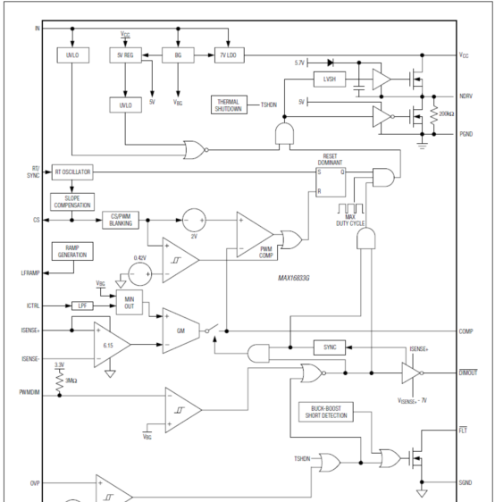
图2. MAX16833G功能框图
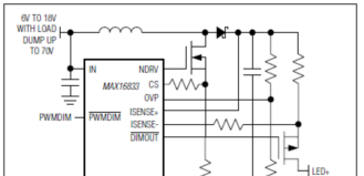
图3. MAX16833简化工作电路
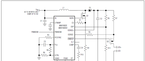
图4. MAX16833/C应用电路图
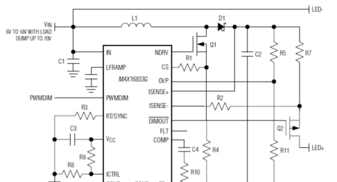
图5. MAX16833G应用电路图
评估板MAX16833 EVK
The MAX16833 evaluation kit (EV kit) provides a proven design to evaluate the MAX16833 high-voltage HB LED driver with integrated high-side current sense. The EV kit is set up for boost and buck-boost configurations and operates from a 5V to 18V DC supply voltage. The EV kit is configured to deliver up to 1A to one string of LEDs. The total voltage of the string can vary from 3V to 36V. The anode of the LED string should be connected to the LED+ terminal. The cathode of the LED string can be connected either to the PGND (boost mode) or LED- (buck-boost mode) terminal. In the case of the boost mode, the input voltage should not exceed the LED string voltage.
The EV kit PCB comes with a MAX16833AUE+ installed, which is the frequency-dithering version. The EV kit also comes with the pin-compatible MAX16833BAUE+, which is the reference-voltage output version.
评估板MAX16833 EVK主要特性:
S Configured for Boost and Buck-Boost
S Analog Dimming Control
S Proven PCB Layout
S Fully Assembled and Tested
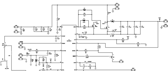
图6. 评估板MAX16833 EVK电路图
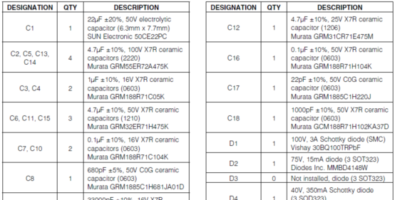
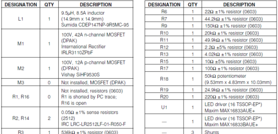
评估板MAX16833 EVK材料清单:
详情请见:
责任编辑:HanFeng
【免责声明】
1、本文内容、数据、图表等来源于网络引用或其他公开资料,版权归属原作者、原发表出处。若版权所有方对本文的引用持有异议,请联系拍明芯城(marketing@iczoom.com),本方将及时处理。
2、本文的引用仅供读者交流学习使用,不涉及商业目的。
3、本文内容仅代表作者观点,拍明芯城不对内容的准确性、可靠性或完整性提供明示或暗示的保证。读者阅读本文后做出的决定或行为,是基于自主意愿和独立判断做出的,请读者明确相关结果。
4、如需转载本方拥有版权的文章,请联系拍明芯城(marketing@iczoom.com)注明“转载原因”。未经允许私自转载拍明芯城将保留追究其法律责任的权利。
拍明芯城拥有对此声明的最终解释权。
相关资讯
:
基于MC33771主控芯片的新能源锂电池管理系统解决方案

AMIC110 32位Sitara ARM MCU开发方案

基于AMIC110多协议可编程工业通信处理器的32位Sitara ARM MCU开发方案

基于展讯SC9820超低成本LTE芯片平台的儿童智能手表解决方案

基于TI公司的AM437x双照相机参考设计

基于MTK6580芯片的W2智能手表解决方案


 2012- 2022 拍明芯城ICZOOM.com 版权所有 客服热线:400-693-8369 (9:00-18:00)


