


 产品分类
产品分类
基于ADI公司的ADP5014四路高性能低噪声降压调节器解决方案
 178
178
 拍明
拍明
原标题:ADI ADP5014四路高性能低噪声降压调节器解决方案
ADI公司的ADP5014是在6 mm × 6 mm 40引脚LFCSP封装中集成四路高性能低噪声降压调节器,其所有通道均集成高端和低端功率金属氧化物半导体场效应晶体管(MOSFET).通道1和通道2同时提供2 A或4 A的可编程输出电流,通道3和通道4同时提供1 A和2 A的可编程输出电流.其它特性包括可选强制脉冲宽度调制(FPWM)/省电模式(PSM),欠压输出(UVO),有源输出放电和电源良好指示.安全特性包括输入欠压闭锁(UVLO),过压保护(OVP),过流保护(OCP)和热关断(TSD).输入电压2.75V-6.0V,可编输出电压0.5V-0.9xVINx.主要用在RF收发器,高速模数转换器(ADC)/数模转换器(DAC),混合信号ASIC,现场可编程门阵列(FPGA)和处理器应用,安防和监控以及医疗应用.本文介绍了ADP5014主要特性,功能框图,典型应用电路,以及评估板ADP5014-EVALZ主要特性,电路图,材料清单和PCB设计图.
The ADP5014 combines four high performance, low noise buckregulators in a 40-lead LFCSP package. Relying on its lowoutput noise (~25 μVrms when VOUT ≤ VREF), the low noisebuck regulator enables the powering up of the noise sensitivesignal chain products.
All channels in the ADP5014 integrate high-side and low-sidepower metal-oxide semiconductor field effect transistors(MOSFET). Channel 1 and Channel 2 deliver a programmableoutput current of 2 A or 4 A. Combining Channel 1 andChannel 2 in a parallel configuration provides a single outputwith up to 8 A of current.
Channel 3 and Channel 4 deliver a programmable output currentof 1 A or 2 A. Combining Channel 3 and Channel 4 in a parallelconfiguration can provide a single output with up to 4 A of current.
The ADP5014 features two enable modes. The manual modehas four individual precision enable pins to enable eachregulator manually. Alternatively, the sequence mode has one grouped precision enable signal with programmable power-upand power-down delay timers on each rail for specific railsequence requirements.
The switching frequency of the ADP5014 can be programmedor synchronized to an external clock from 500 kHz to 2.5 MHz.The ADP5014 offers other key features like selective forcedpulse width modulation (FPWM)/power saving mode (PSM),an undervoltage output (UVO), active output discharge, and apower-good flag. Other safety features include input undervoltagelockout (UVLO), overvoltage protection (OVP),overcurrent protection (OCP) and thermal shutdown (TSD).
ADP5014主要特性:
Input voltage range: 2.75 V to 6.0 V
Programmable output voltage range: 0.5 V to 0.9 × PVINx
Low output noise: ~25 μVrms when VOUT ≤ VREF±1.0% output accuracy over full temperature range500 kHz to 2.5 MHz adjustable switching frequency
Power regulation
Channel 1 and Channel 2: programmable 2 A/4 A syncbuck regulators, or single 8 A output in parallel
Channel 3 and Channel 4: programmable 1 A/2 A syncbuck regulators, or single 4 A output in parallel
Flexible parallel operation
Precision enable with 0.6 V threshold
Manual or sequence mode for power-up and power-downsequence
Selective FPWM or PSM operation mode
Precision undervoltage comparator
Frequency synchronization input or output
Active output discharge switch
Power-good flag on selective channels via factory fuse
UVLO, OVP, OCP, and TSD protection
40-lead, 6 mm × 6 mm LFCSP package
−40 ℃ to +125 ℃ junction temperature
ADP5014应用:
RF transceiver, high speed analog-to-digital converter
(ADC)/digital-to-analog converter (DAC), mixed signal ASIC
FPGA and processor applications
Security and surveillance
Medical applications
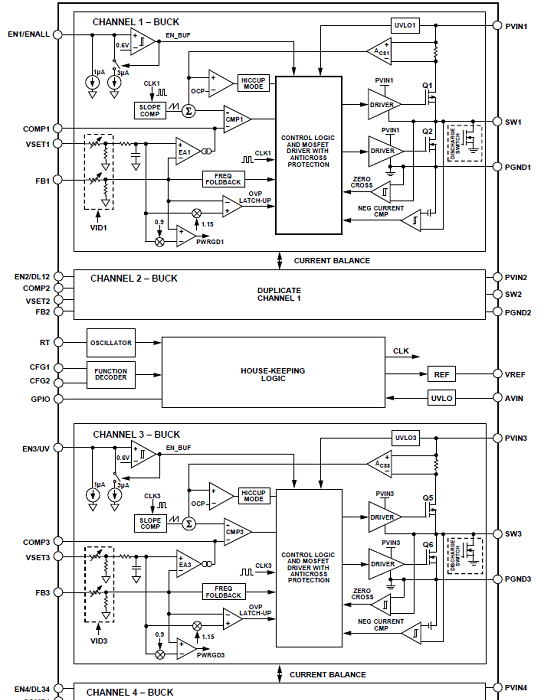
ADP5014功能框图
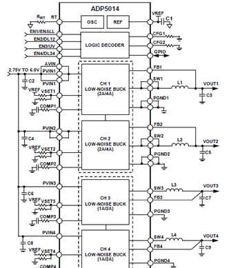
图2. ADP5014典型应用电路图(1)
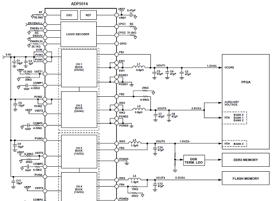
图3. ADP5014典型应用电路图(2):FPGA应用,1.2MHz开关频率,顺序使能模式
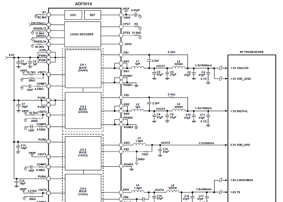
图4. ADP5014典型应用电路图(2):RF收发器应用,1.2MHz开关频率,顺序使能模式
评估板ADP5014-EVALZ
This user guide describes the evaluation of the ADP5014 and includes detailed schematics and printed circuit board (PCB) layouts.
The ADP5014-EVALZ evaluation board combines four high performance buck regulators in a 40-lead LFCSP package to meet the demanding performance and board space requirements.
Full details on the ADP5014 regulator are provided in the ADP5014 data sheet, available from Analog Devices, Inc. Consult the data sheet in conjunction with this user guide when working with this evaluation board.
评估板ADP5014-EVALZ主要特性:
Full featured evaluation board for the ADP5014
Compact solution size
4-layer high glass transition temperature (TG) PCB for superior thermal performance
Convenient connections through vertical printed circuit tail pin headers
Supply voltage
2.75 V to 6.0 V for PVINx
Mode option to select manual or sequence enable
Mode option to select PSM or FPWM operation
Programmable switching frequency from 500 kHz to 2.5 MHz
Frequency synchronization input or output
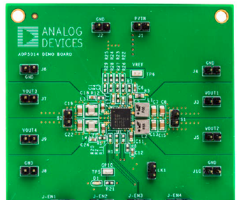
图5.评估板ADP5014-EVALZ外形图
评估板ADP5014-EVALZ材料清单(BOM):
优势和特点
输入电压范围:2.75 V至6.0 V
可编程输出电压范围:0.5 V至0.9 × PVINx
低输出噪声:~25 μV rms(VOUT ≤ VREF时)
输出精度:±1.0%(整个温度范围内)
可调开关频率范围:500 kHz至2.5 MHz
功率调节
通道1和通道2:可编程2 A/4 A同步降压稳压器,或单通道8 A输出(并联使用)
通道3和通道4:可编程1 A/2 A同步降压稳压器,或单通道4 A输出(并联使用)
灵活的并行操作
精密使能,0.6 V阈值
用于上电和关断时序的手动或序列模式
可选FPWM或PSM工作模式
精密欠压比较器
频率同步输入或输出
有源输出放电开关
可选通道通过工厂熔断器提供电源良好指示
UVLO、OVP、OCP和TSD保护
40引脚、6 mm × 6 mm LFCSP封装
结温范围:-40°C至+125°C
ADP5014在一个40引脚LFCSP封装中集成四个高性能、低噪声降压稳压器。依赖其低输出噪声性能(~25 μV rms,VOUT ≤ VREF时),低噪声降压稳压器可为噪声敏感型信号链产品上电。
ADP5014中的所有通道均集成高端和低端功率金属氧化物半导体场效应晶体管(MOSFET)。通道1和通道2同时提供2 A或4 A的可编程输出电流。以并联配置方式组合通道1和通道2可提供高达8 A的单路输出电流。
通道3和通道4同时提供1 A和2 A的可编程输出电流。以并联配置方式组合通道3和通道4可提供高达4 A的单路输出电流。
ADP5014具有两种使能模式。手动模式具有四个独立精密使能引脚,可手动使能各调节器。或者,序列模式具有一个分组的精密使能信号,在各供电轨上集成可编程上电和关断延迟定时器,可满足特定的供电轨时序要求。
ADP5014的开关频率可编程或同步至500 kHz至2.5 MHz的外部时钟。
ADP5014提供其它主要特性,如可选强制脉冲宽度调制(FPWM)/省电模式(PSM)、欠压输出(UVO)、有源输出放电和电源良好指示。其它安全特性包括输入欠压闭锁(UVLO)、过压保护(OVP)、过流保护(OCP)和热关断(TSD)。
应用
RF收发器、高速模数转换器(ADC)/数模转换器(DAC)、混合信号ASIC
现场可编程门阵列(FPGA)和处理器应用
安防和监控
医疗应用
责任编辑:HanFeng
【免责声明】
1、本文内容、数据、图表等来源于网络引用或其他公开资料,版权归属原作者、原发表出处。若版权所有方对本文的引用持有异议,请联系拍明芯城(marketing@iczoom.com),本方将及时处理。
2、本文的引用仅供读者交流学习使用,不涉及商业目的。
3、本文内容仅代表作者观点,拍明芯城不对内容的准确性、可靠性或完整性提供明示或暗示的保证。读者阅读本文后做出的决定或行为,是基于自主意愿和独立判断做出的,请读者明确相关结果。
4、如需转载本方拥有版权的文章,请联系拍明芯城(marketing@iczoom.com)注明“转载原因”。未经允许私自转载拍明芯城将保留追究其法律责任的权利。
拍明芯城拥有对此声明的最终解释权。
相关资讯
:
基于MC33771主控芯片的新能源锂电池管理系统解决方案

AMIC110 32位Sitara ARM MCU开发方案

基于AMIC110多协议可编程工业通信处理器的32位Sitara ARM MCU开发方案

基于展讯SC9820超低成本LTE芯片平台的儿童智能手表解决方案

基于TI公司的AM437x双照相机参考设计

基于MTK6580芯片的W2智能手表解决方案


 2012- 2022 拍明芯城ICZOOM.com 版权所有 客服热线:400-693-8369 (9:00-18:00)


