模块板卡:基于STM32F407ZGT6和EP4CE10E22C8芯片的双核心工控板解决方案(PCBA)
 405
405
 拍明
拍明
原标题:双核心工控板
应用领域:工业电子
方案类型:模块板卡
方案概述
应用领域:工业控制
应用场景:采用STM32 和Cyclone FPGA并行处理器的双核工控板,具备较强的计算能力和数据交换能力,适用于运动控制和步进电机控制端口
交付形式:PCBA
性能参数:
l 主芯片:采用ARM+FPGA双核,其中ARM采用的是STM32F407ZGT6,主频168MHz,Cortex-M4内核;FPGA采用114脚Cyclone四代EP4CE10E22C8
l 256K非易失性铁电存储器FM1808,无限次读写次数
l ARM扩展IO数目为31个,FPGA扩展IO数目为40个
l 预留4路步进电机驱动接口
l 1路工业CAN总线控制接口
l 6路串口通信接口,可扩展蓝牙、Zigbee等功能
l 3路编码器信号接口
l 7路小功率驱动信号(500mA)接口
l 支持OLED显示模块
l 5路AD输入接口,2路DA输出接口
l 支持RS485总线
l 1路高速USB接口
方案图片:
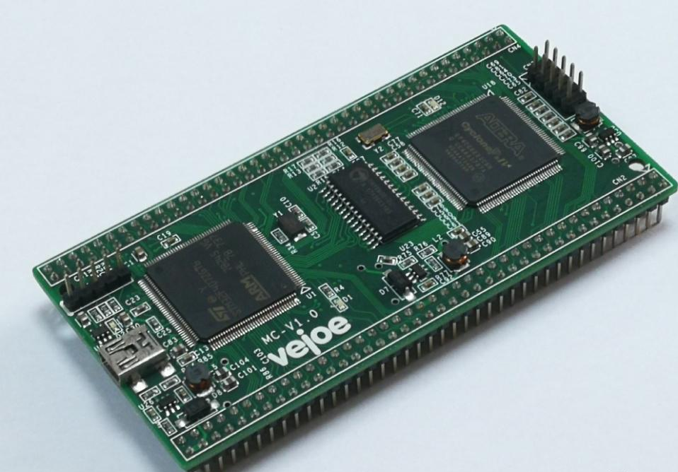
【STM32F407ZGT6】
High-performance foundation line, ARM Cortex-M4 core with DSP and FPU, 1 Mbyte Flash, 168 MHz CPU, ART Accelerator, Ethernet, FSMC
The STM32F405xx and STM32F407xx family is based on the high-performance ARM®Cortex®-M4 32-bit RISC core operating at a frequency of up to 168 MHz. The Cortex-M4 core features a Floating point unit (FPU) single precision which supports all ARM single-precision data-processing instructions and data types. It also implements a full set of DSP instructions and a memory protection unit (MPU) which enhances application security.
The STM32F405xx and STM32F407xx family incorporates high-speed embedded memories (Flash memory up to 1 Mbyte, up to 192 Kbytes of SRAM), up to 4 Kbytes of backup SRAM, and an extensive range of enhanced I/Os and peripherals connected to two APB buses, three AHB buses and a 32-bit multi-AHB bus matrix.
All devices offer three 12-bit ADCs, two DACs, a low-power RTC, twelve general-purpose 16-bit timers including two PWM timers for motor control, two general-purpose 32-bit timers. a true random number generator (RNG). They also feature standard and advanced communication interfaces.
Key Features
Core: ARM®32-bit Cortex®-M4 CPU with FPU, Adaptive real-time accelerator (ART Accelerator™) allowing 0-wait state execution from Flash memory, frequency up to 168 MHz, memory protection unit, 210 DMIPS/1.25 DMIPS/MHz (Dhrystone 2.1), and DSP instructions
Memories
Up to 1 Mbyte of Flash memory
Up to 192+4 Kbytes of SRAM including 64-Kbyte of CCM (core coupled memory) data RAM
Flexible static memory controller supporting Compact Flash, SRAM, PSRAM, NOR and NAND memories
LCD parallel interface, 8080/6800 modes
Clock, reset and supply management
1.8 V to 3.6 V application supply and I/Os
POR, PDR, PVD and BOR
4-to-26 MHz crystal oscillator
Internal 16 MHz factory-trimmed RC (1% accuracy)
32 kHz oscillator for RTC with calibration
Internal 32 kHz RC with calibration
Sleep, Stop and Standby modes
VBATsupply for RTC, 20×32 bit backup registers + optional 4 KB backup SRAM
3×12-bit, 2.4 MSPS A/D converters: up to 24 channels and 7.2 MSPS in triple interleaved mode
2×12-bit D/A converters
General-purpose DMA: 16-stream DMA controller with FIFOs and burst support
Up to 17 timers: up to twelve 16-bit and two 32-bit timers up to 168 MHz, each with up to 4 IC/OC/PWM or pulse counter and quadrature (incremental) encoder input
Debug mode
Serial wire debug (SWD) & JTAG interfaces
Cortex-M4 Embedded Trace Macrocell™
Up to 140 I/O ports with interrupt capability
Up to 136 fast I/Os up to 84 MHz
Up to 138 5 V-tolerant I/Os
Up to 15 communication interfaces
Up to 3 × I2C interfaces (SMBus/PMBus)
Up to 4 USARTs/2 UARTs (10.5 Mbit/s, ISO 7816 interface, LIN, IrDA, modem control)
Up to 3 SPIs (42 Mbits/s), 2 with muxed full-duplex I2S to achieve audio class accuracy via internal audio PLL or external clock
2 × CAN interfaces (2.0B Active)
SDIO interface
Advanced connectivity
USB 2.0 full-speed device/host/OTG controller with on-chip PHY
USB 2.0 high-speed/full-speed device/host/OTG controller with dedicated DMA, on-chip full-speed PHY and ULPI
10/100 Ethernet MAC with dedicated DMA: supports IEEE 1588v2 hardware, MII/RMII
8- to 14-bit parallel camera interface up to 54 Mbytes/s
True random number generator
CRC calculation unit
96-bit unique ID
RTC: subsecond accuracy, hardware calendar
【EP4CE10E22C8】
Altera’s new Cyclone® IV FPGA device family extends the Cyclone FPGA seriesleadership in providing the market’s lowest-cost, lowest-power FPGAs, now with atransceiver variant. Cyclone IV devices are targeted to high-volume, cost-sensitiveapplications, enabling system designers to meet increasing bandwidth requirementswhile lowering costs.
Built on an optimized low-power process, the Cyclone IV device family offers thefollowing two variants:
■ Cyclone IV E—lowest power, high functionality with the lowest cost
■ Cyclone IV GX—lowest power and lowest cost FPGAs with 3.125 Gbps
transceivers
1 Cyclone IV E devices are offered in core voltage of 1.0 V and 1.2 V.
f For more information, refer to the Power Requirements for Cyclone IV Devices chapter.
Providing power and cost savings without sacrificing performance, along with alow-cost integrated transceiver option, Cyclone IV devices are ideal for low-cost,
small-form-factor applications in the wireless, wireline, broadcast, industrial,consumer, and communications industries.
Cyclone IV Device Family Features
The Cyclone IV device family offers the following features:
■ Low-cost, low-power FPGA fabric:
■ 6K to 150K logic elements
■ Up to 6.3 Mb of embedded memory
■ Up to 360 18 × 18 multipliers for DSP processing intensive applications
■ Protocol bridging applications for under 1.5 W total power
■ Cyclone IV GX devices offer up to eight high-speed transceivers that provide:
■ Data rates up to 3.125 Gbps
■ 8B/10B encoder/decoder
■ 8-bit or 10-bit physical media attachment (PMA) to physical coding sublayer(PCS) interface
■ Byte serializer/deserializer (SERDES)
■ Word aligner
■ Rate matching FIFO
■ TX bit slipper for Common Public Radio Interface (CPRI)
■ Electrical idle
■ Dynamic channel reconfiguration allowing you to change data rates andprotocols on-the-fly
■ Static equalization and pre-emphasis for superior signal integrity
■ 150 mW per channel power consumption
■ Flexible clocking structure to support multiple protocols in a single transceiverblock
■ Cyclone IV GX devices offer dedicated hard IP for PCI Express (PIPE) (PCIe)Gen 1:
■ ×1, ×2, and ×4 lane configurations
■ End-point and root-port configurations
■ Up to 256-byte payload
■ One virtual channel
■ 2 KB retry buffer
■ 4 KB receiver (Rx) buffer
■ Cyclone IV GX devices offer a wide range of protocol support:
■ PCIe (PIPE) Gen 1 ×1, ×2, and ×4 (2.5 Gbps)
■ Gigabit Ethernet (1.25 Gbps)
■ CPRI (up to 3.072 Gbps)
■ XAUI (3.125 Gbps)
■ Triple rate serial digital interface (SDI) (up to 2.97 Gbps)
■ Serial RapidIO (3.125 Gbps)
■ Basic mode (up to 3.125 Gbps)
■ V-by-One (up to 3.0 Gbps)
■ DisplayPort (2.7 Gbps)
■ Serial Advanced Technology Attachment (SATA) (up to 3.0 Gbps)
■ OBSAI (up to 3.072 Gbps)
■ Up to 532 user I/Os
■ LVDS interfaces up to 840 Mbps transmitter (Tx), 875 Mbps Rx
■ Support for DDR2 SDRAM interfaces up to 200 MHz
■ Support for QDRII SRAM and DDR SDRAM up to 167 MHz
■ Up to eight phase-locked loops (PLLs) per device
■ Offered in commercial and industrial temperature grades
责任编辑:David
【免责声明】
1、本文内容、数据、图表等来源于网络引用或其他公开资料,版权归属原作者、原发表出处。若版权所有方对本文的引用持有异议,请联系拍明芯城(marketing@iczoom.com),本方将及时处理。
2、本文的引用仅供读者交流学习使用,不涉及商业目的。
3、本文内容仅代表作者观点,拍明芯城不对内容的准确性、可靠性或完整性提供明示或暗示的保证。读者阅读本文后做出的决定或行为,是基于自主意愿和独立判断做出的,请读者明确相关结果。
4、如需转载本方拥有版权的文章,请联系拍明芯城(marketing@iczoom.com)注明“转载原因”。未经允许私自转载拍明芯城将保留追究其法律责任的权利。
拍明芯城拥有对此声明的最终解释权。


 产品分类
产品分类




 2012- 2022 拍明芯城ICZOOM.com 版权所有 客服热线:400-693-8369 (9:00-18:00)


