ADI AD7768-1F 24位Σ-Δ模拟数转换器(ADC)解决方案
 475
475
 拍明
拍明
原标题:ADI AD7768-1F 24位Σ-Δ模拟数转换器(ADC)解决方案
ADI公司的ad7768-1F是低功耗高性能24位Σ-Δ模拟数转换器(ADC),集成了Σ-Δ调制器和数字滤波器,以用于AC和DC信号的精密转换,动态范围108.5dB,失调误差±30 μV,增益误差±30 ppm, INL±1.1 ppm,低波纹FIR 带宽(BW)为DC到110.8kHz,适用于单路低功耗数据收集系统(DAQ)设计,主要用在仪器和传感器类型,声音和振动,声学和材料科学研究和开发,闭环验证的控制和硬件,电测试和测量,音频测试以及电压与电流测量,门诊EEG,EMG和EGG生命体征监测,基于USB,PXI和以太网的模块DAQ,以及通路隔离的模块DAQ设计.本文介绍了AD7768-1F主要特性,功能框图已以及评估板EV-AD7768-1FMCZ主要特性,电路图,材料清单和PCB设计图.
The AD7768-1 is a low power, high performance, Σ-Δ analog-to-digital converter (ADC), with a Σ-Δ modulator and digital filter for precision conversion of both ac and dc signals. The AD7768-1 is a single-channel version of the AD7768, an 8-channel, simultaneously sampling, Σ-Δ ADC. The AD7768-1 provides a single configurable and reusable data acquisition (DAQ) footprint, which establishes a new industry standard in combined ac and dc performance and enables instrumentation and industrial system designers to design across multiple measurement variants for both isolated and nonisolated applications.
The AD7768-1 achieves a 108.5 dB dynamic range when using the low ripple, finite impulse response (FIR) digital filter at 256 kSPS, giving 110.8 kHz input bandwidth (BW), combined with ±1.1 ppm integral nonlinearity (INL), ±30 μV offset error, and ±30 ppm gain error.A wider bandwidth, up to 500 kHz Nyquist (filter −3 dB point of 204 kHz), is available using the sinc5 filter, enabling a view of signals over an extended range.
The AD7768-1 offers the user the flexibility to configure and optimize for input bandwidth vs. output data rate (ODR) and vs. power dissipation. The flexibility of the AD7768-1 allows dynamic analysis of a changing input signal, making the device particularly useful in general-purpose DAQ systems. The selection of one of three available power modes allows the designer to achieve required noise targets while minimizing power consumption. The design of the AD7768-1 is unique in that it becomes a reusable and flexible platform for low power dc and high performance ac measurement modules.
The AD7768-1 achieves the optimum balance of dc and ac performance with excellent power efficiency. The following three operating modes allow the user to trade off the input bandwidth vs. power budgets:
• Fast mode offers both a sinc filter with up to 256 kSPS and 52.2 kHz of bandwidth, and 26.4 mW of power consumption, or a FIR filter with up to 256 kSPS, 110.8 kHz of bandwidth and 36.8 mW of power consumption.
• Median mode offers a FIR filter with up to 128 kSPS, 55.4 kHz of bandwidth and 19.7 mW of power consumption.
• Low power mode offers a FIR filter with up to 32 kSPS, 13.85 kHz of bandwidth and 6.75 mW of power consumption.
The AD7768-1 offers extensive digital filtering capabilities that meet a wide range of system requirements. The filter options allow configuration for frequency domain measurements withtight gain error over frequency, linear phase response requirements (brick wall filter), a low latency path (sinc5 or sinc3) for use in control loop applications, and measuring dc inputs with the ability to configure the sinc3 filter to reject the line frequency of either 50 Hz or 60 Hz. All filters offer programmable decimation.
A 1.024 MHz sinc5 filter path exists for users seeking an even higher ODR than is achievable using the low ripple FIR filter. This path is quantization noise limited. Therefore, it is best suited for customers requiring minimum latency for control loops or implementing custom digital filtering on an external field programmable gate array (FPGA) or digital signal processor (DSP).
The filter options include the following:
• A low ripple FIR filter with a ±0.005 dB pass-band ripple to 102.4 kHz.
• A low latency sinc5 filter with up to a 1.024 MHz data rate to maximize control loop responsiveness.
• A low latency sinc3 filter that is fully programmable, with 50 Hz/60 Hz rejection capabilities.
When using the AD7768-1, embedded analog functionality within the AD7768-1 greatly reduces the design burden over the entire application range. The precharge buffer on each analog input decreases the analog input current compared to competing products, simplifying the task of an external amplifier to drive the analog input.
A full buffer input on the reference reduces the input current, providing a high impedance input for the external reference device or in buffering any reference sense resistor scenarios used in ratiometric measurements.
The device operates with a 5.0 V AVDD1 − AVSS supply, a 2.0 V to 5.0 V AVDD2 − AVSS supply, and a 1.8 V to 3.3 V IOVDD − DGND supply.
In low power mode, the AVDD1, AVDD2, and IOVDD supplies can run from a single 3.3 V rail.
The device requires an external reference. The absolute input reference (REFIN) voltage range is 1 V to AVDD1 − AVSS.The specified operating temperature range is −40 ℃ to +125℃. The device is housed in a 4 mm × 5 mm, 28-lead LFCSP.
Note that, throughout this data sheet, multifunction pins, such as XTAL2/MCLK, are referred to either by the entire pin name or by a single function of the pin, for example, MCLK, when only that function is relevant.
AD7768-1F主要特性:
ADC for single-channel low power, platform DAQ designs
Wide BW
Sinc filter BW range: DC to 204 kHz
Low ripple FIR BW range: DC to 110.8 kHz
Precision ac and dc performance
108.5 dB dynamic range
−120 dB THD
±1.1 ppm of FSR INL, ±30 μV offset error, ±30 ppm of FSR gain error
Programmable ODR, filter type, and latency
ODR values up to 1024 kSPS
Linear phase digital filter options
Low ripple FIR filter: ±0.005 dB maximum pass-band ripple, dc to 102.4 kHz
Low latency sinc5 filter
Low latency sinc3 filter enabling 50 Hz/60 Hz rejection
Programmable power consumption and bandwidth
Fast, highest speed
52.224 kHz BW, 26.4 mW (sinc5 filter)
110.8 kHz BW, 36.8 mW (FIR filter)
Median, half speed: 55.4 kHz BW, 19.7 mW (FIR filter)
Low power, low speed: 13.9 kHz BW, 6.75 mW (FIR filter)
Power supply
AVDD1 − AVSS = 5.0 V typical
AVDD2 − AVSS = 2.0 V to 5.0 V typical
Analog supplies can run from split supply (true bipolar)
IOVDD − DGND = 1.8 V to 3.3 V typical
Low power mode can run from single 3.3 V supply
Pin control or SPI interface configurable
Suite of diagnostic check mechanisms
Temperature, interface CRC, and memory map CRC
Package: 28-lead, 4 mm × 5 mm, LFCSP
Temperature range: −40℃ to +125℃
AD7768-1F应用:
Platform ADC to serve a superset of measurements and sensor types
Sound and vibration, acoustic, and material science research and development
Control and hardware in loop verification
Condition monitoring for predictive maintenance
Electrical test and measurement
Audio testing and current and voltage measurement
Clinical EEG, EMG, and ECG vital signs monitoring
USB-, PXI-, and Ethernet-based modular DAQ
Channel to channel isolated modular DAQ designs
评估板EV-AD7768-1FMCZ
The EV-AD7768-1FMCZ evaluation kit features the AD7768-1 24-bit, 256 kSPS analog-to-digital converter (ADC). The EV-AD7768-1FMCZ board connects to the USB port of the PC via the EVAL-SDP-CH1Z motherboard. By default, power is supplied from the EVAL-SDP-CH1Z supply, which is regulated to 5 V and 3.3 V to supply the AD7768-1 and support components.
The EV-AD7768-1FMCZ software fully configures the AD7768-1 device register functionality and provides dc and ac time domain analysis in the form of waveform graphs, histograms, and associated noise analysis for ADC performance evaluation.
The EV-AD7768-1FMCZ is an evaluation board that allows the user to evaluate the features of the ADC. The user PC software executable controls the AD7768-1 over USB through the system demonstration platform (EVAL-SDP-CH1Z).
评估板EV-AD7768-1FMCZ主要特性:
Full featured evaluation board for the AD7768-1
PC control in conjunction with EVAL-SDP-CH1Z
PC software control and data analysis
Time and frequency domain
Standalone hardware capability
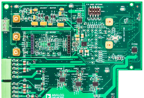
图.评估板EV-AD7768-1FMCZ外形图
责任编辑:HanFeng
【免责声明】
1、本文内容、数据、图表等来源于网络引用或其他公开资料,版权归属原作者、原发表出处。若版权所有方对本文的引用持有异议,请联系拍明芯城(marketing@iczoom.com),本方将及时处理。
2、本文的引用仅供读者交流学习使用,不涉及商业目的。
3、本文内容仅代表作者观点,拍明芯城不对内容的准确性、可靠性或完整性提供明示或暗示的保证。读者阅读本文后做出的决定或行为,是基于自主意愿和独立判断做出的,请读者明确相关结果。
4、如需转载本方拥有版权的文章,请联系拍明芯城(marketing@iczoom.com)注明“转载原因”。未经允许私自转载拍明芯城将保留追究其法律责任的权利。
拍明芯城拥有对此声明的最终解释权。


 产品分类
产品分类




 2012- 2022 拍明芯城ICZOOM.com 版权所有 客服热线:400-693-8369 (9:00-18:00)


