


 产品分类
产品分类
基于Microsemi公司的PolarFire第五代非易失FPGA系列开发方案
 201
201
 拍明
拍明
原标题:MicrosemiPolarFire第五代非易失FPGA系列开发方案
Microsemi公司的PolarFire FPGA是第五代非易失FPGA器件,采用最新的28nm非易失工艺技术,具有中等密度和最低功耗,集成了最低功耗的FPGA架构,最低功耗的12.7Gbps收发器,内置低功耗双路PCI Express Gen2 (EP/RP),以及可选择数据安全器件和集成低功耗加密协处理器.多达481K逻辑单元,工作电压1.0V-1.05V,工作温度商用(0℃- 100℃),工业用(-40℃ - 100℃)主要用在通信,工业,航空航天和国防市场.本文介绍了PolarFire FPGA主要特性,低功耗特性,可靠特性和安全特性,框图,以及PolarFire FPGA评估板硬件特性,框图,电路图和元件表以及PCB元件布局图.
PolarFire™ FPGAs are the fifth-generation family of non-volatile FPGA devices from Microsemi, built onstate-of-the-art 28nm non-volatile process technology. Cost-optimized PolarFire FPGAs deliver thelowest power at mid-range densities. PolarFire FPGAs lower the cost of mid-range FPGAs by integratingthe industry’s lowest power FPGA fabric, lowest power 12.7 Gbps transceiver lane, built-in low powerdual PCI Express Gen2 (EP/RP), and, on select data security (S) devices, an integrated low-power cryptoco-processor. PolarFire FPGAs can operate at 1.0 V and 1.05 V, offering the end user the ability to tradeoff power and performance to match the application requirements.This document describes the features of PolarFire FPGA extended commercial (0℃ to 100℃) andindustrial (–40℃ to 100℃) device offerings.
PolarFire FPGA主要特性:
Up to 481K logic elements consisting of a 4-input look-up table (LUT) with a fractureable D-type flipflop20 Kb dual- or two-port large static random access memory (LSRAM) block with built-in single errorcorrect double error detect (SECDED)
64 × 12 two-port μRAM block implemented as an array of latches
18 × 18 math block with a pre-adder, a 48-bit accumulator, and an optional 16 deep x 18 coefficientROM
Built-in μPROM, modifiable at program time, readable at run time for user data storage
High-speed serial connectivity with built-in multi-gigabit multi-protocol transceivers from 250 Mbpsto 12.7 Gbps
Integrated dual PCIe for up to ×4 Gen2 endpoint (EP) and root port (RP) designs
High-speed I/O (HSIO) supporting up to 1600 Mbps DDR4, 1333 Mbps DDR3L, and 1333 Mbps
LPDDR3/DDR3 memories with integrated I/O digital
General purpose I/O (GPIO) supporting 3.3 V, built-in CDR for serial gigabit Ethernet, 1067 Mbps
DDR3, and 1250 Mbps LVDS I/O speed with integrated I/O digital logic
Low-power phase-locked loops (PLLs) and delay-locked loops (DLLs) for high precision and low-jitterV and 1.05 V operating modes
PolarFire FPGA低功耗特性:
Low device static power
Low inrush current
Low power transceivers
Unique Flash*Freeze (F*F) mode
PolarFire FPGA可靠特性:
FPGA configuration cells single event upset (SEU) immune
Built-in SECDED and memory interleaving on LSRAMs
System controller suspend mode for safety-critical designs
PolarFire FPGA安全特性:
Cryptography Research Incorporated (CRI)-patented differential power analysis (DPA) bitstreamprotection
Integrated physically unclonable function (PUF)
56 KBytes of secure non-volatile memory (sNVM)
Built-in tamper detectors and countermeasures
Digest integrity check for FPGA, μPROM, and sNVM
Data security features in S devices—true random number generator, integrated Athena TeraFire
EXP5200B Crypto Coprocessor, suite B capable, and CRI DPA countermeasure pass-through license
Libero® SoCPolarFire FPGA Toolset
Complete FPGA and embedded software development environment
Includes Synplify Pro synthesis and Mentor ModelSim ME simulation
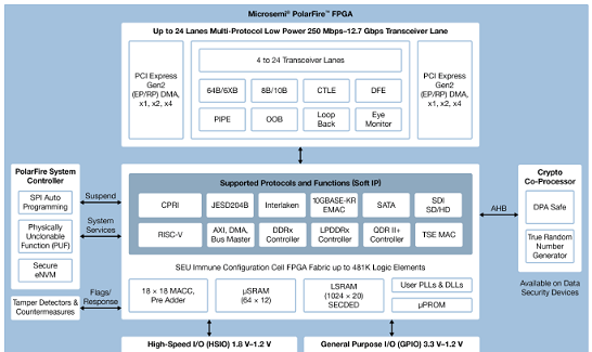
图1.PolarFire FPGA框图
PolarFire FPGA评估板
Microsemi’sPolarFire Evaluation Kit offers high-performance evaluation across a broad class of applications. This kit is ideally suited for high-speed transceiver evaluation, 10Gb Ethernet, IEEE1588, JESD204B, SyncE, CPRI and more. The kit connections include a high pin count (HPC) FPGA mezzanine card (FMC), numerous SMAs, PCIe, Dual Gigabit Ethernet RJ45, SFP+ and USB. A 300K logic element (LE) PolarFire FPGA with DDR4, DDR3 and SPI-flash allow a broad class of high-performance designs to be developed.
PolarFire FPGA评估板硬件特性:
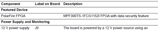
300K LE PolarFire FPGA in an FCG1152 Package (MPF300TS-1FCG1152EES)
HPC FMC Connector
1x SFP+ Cage
IEEE1588 PLL
SMA connectors for testing of full-duplex 12.7Gbps SERDES channel
4GB DDR4 x32 and 2GB DDR3 x16
PCI Express (x4) Edge Connector
2 x RJ45 for 10/100/1000 Ethernet using SGMII on GPIO
Dual 10/100/1000BASE-T PHY (VSC8575) for SyncE and 1588 application
SATA Interface
Power Management Unit for 1 or 1.05v PolarFire FPGA core voltage
USB to UART Interface
Embedded programming and debugging using SPI and JTAG
On-board Power Monitoring
2 x 1Gb SPI Flash Memory
The MicrosemiPolarFire™ FPGA Evaluation Kit (MPF300-EVAL-KIT), which is RoHS-compliant,enables you to evaluate the PolarFire family of FPGAs with support for the following interfaces:
• PCI Express Gen1 and Gen2
• 1 GbE
• DDR3 and DDR4 memory
• FMC HPC with 8 Transceiver lanes
• 1 Full-Duplex Transceiver SMAs
• SFP+ Cage
• UART Interface to FTDI device
• SPI Interface to SPI Flash device
PolarFire FPGA评估板包括:
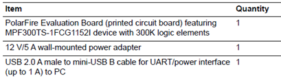
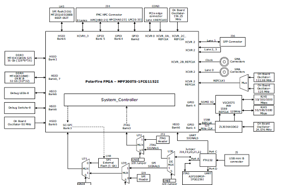
图2.PolarFire FPGA评估板框图
PolarFire FPGA评估板主要特性:
The PolarFire Evaluation Board features the PolarFire MPF300TS-1FCG1152I FPGA. The device hasthe following capabilities:
• 20 Kb dual-port or two-port large static random access memory (LSRAM) block with a built-in singleerror correct double error detect (SECDED)
• 64 × 12 two-port μSRAM block implemented as an array of latches
• 18 × 18 Multiply Accumulate (MACC) block with a pre-adder, a 48-bit accumulator, and an optional16 deep × 18 coefficient RO
• Built-in μPROM, modifiable at program time, readable at run time for user data storage
• Digest integrity check for FPGA, μPROM, and sNVM
• Low-power features:
• Low device static power
• Low inrush current
• Low power transceivers
• Unique Flash*Freeze (F*F) mode
• High-performance communication interfaces
The PolarFire Evaluation Board has several standard interfaces, including:
• VSC8575 with two RJ45 connector for 101001000 Mbps Ethernet
• 8 Full-Duplex Transceiver lanes connected through FMC connector
• FMC HPC connector
• DDR3 memory
• DDR4 memory
• Power Sequence and monitor chip
• x4 Lane PCIe Edge connector
• SFP+ connector
• Two SPI Flash devices
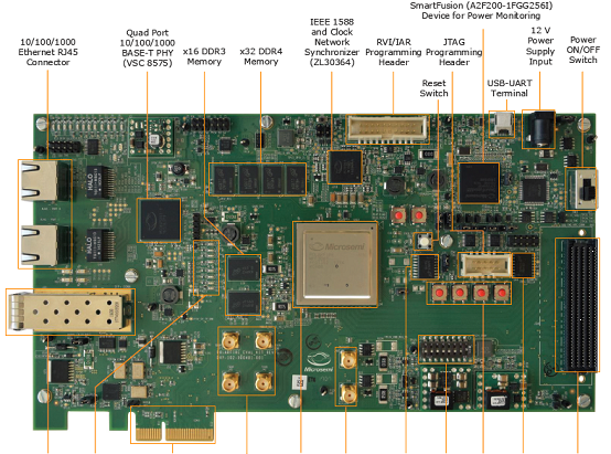
图3.PolarFire FPGA评估板外形图
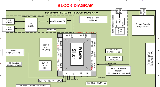
图4.PolarFire FPGA评估板电路图(1)
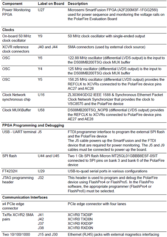
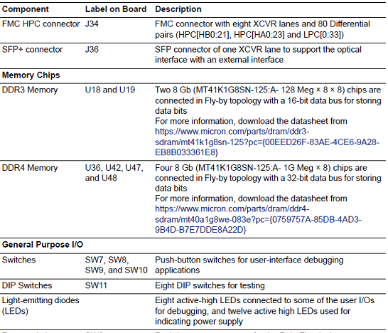
PolarFire FPGA评估板材料元件表:
责任编辑:Davia
【免责声明】
1、本文内容、数据、图表等来源于网络引用或其他公开资料,版权归属原作者、原发表出处。若版权所有方对本文的引用持有异议,请联系拍明芯城(marketing@iczoom.com),本方将及时处理。
2、本文的引用仅供读者交流学习使用,不涉及商业目的。
3、本文内容仅代表作者观点,拍明芯城不对内容的准确性、可靠性或完整性提供明示或暗示的保证。读者阅读本文后做出的决定或行为,是基于自主意愿和独立判断做出的,请读者明确相关结果。
4、如需转载本方拥有版权的文章,请联系拍明芯城(marketing@iczoom.com)注明“转载原因”。未经允许私自转载拍明芯城将保留追究其法律责任的权利。
拍明芯城拥有对此声明的最终解释权。
相关资讯
:
基于MC33771主控芯片的新能源锂电池管理系统解决方案

AMIC110 32位Sitara ARM MCU开发方案

基于AMIC110多协议可编程工业通信处理器的32位Sitara ARM MCU开发方案

基于展讯SC9820超低成本LTE芯片平台的儿童智能手表解决方案

基于TI公司的AM437x双照相机参考设计

基于MTK6580芯片的W2智能手表解决方案


 2012- 2022 拍明芯城ICZOOM.com 版权所有 客服热线:400-693-8369 (9:00-18:00)


