


 产品分类
产品分类
基于NXP公司的S32V234视频处理器开发方案
 372
372
 拍明
拍明
原标题:NXP S32V234视频处理器开发方案
nxp公司的S32V234是第二代视频处理器系列,基于64位ARM Cortex-A53CPU,具有高达1000MHz 四核ARM Cortex-A53,集成了32 KB/32 KB I-/D- L1高速缓存,NEON MPE协处理器,双精度FPU,带2 CPU和256KB L2缓存的2集群,存储器管理单元,GIC中断控制器,提供ISP,功能强大的3D GPU,两个APEX-2可视加速器,支持SafeAssure™安全性,具有汽车级的可靠性,功能安全性,支持汽车和工业自动化,适用于汽车ADAS,NCAP前置摄像头,物体检测和识别,车载全景可视系统以及机器学习和传感器融合应用.本文介绍了S32V234主要特性,框图,评估板SBC-S32V234主要特性和电路图.
The S32V234 is our 2nd generation vision processor family designed to support computation intensive applications for image processing and offers an ISP, powerful 3D GPU, dual APEX-2 vision accelerators, security and supports SafeAssure™.S32V234 is suited for ADAS, NCAP front camera, object detection and recognition, surround view, machine learning and sensor fusion applications. S32V234 is engineered for automotive-grade reliability, functional safety and security measures to support vehicle and industrial automation.
S32V234 has a complete enablement platform supported by S32 Design Studio IDE for Vision which includes a compiler, debugger, Vision SDK, Linux BSP and graph tools.
S32V234主要特性:
• ARM Cortex-A53, 64-bit CPU
– Up to 1000 MHz Quad ARM Cortex-A53
– 32 KB/32 KB I-/D- L1 Cache
– NEON MPE co-processor
– Dual precision FPU
– 2 clusters with 2 CPUs and 256 KB L2 cache each
– Memory Management Unit
– GIC Interrupt Controller
– ECC/parity error support for its memories
– Generic timers
– Fault encapsulation by hardware for redundantexecuted application software on multiple corecluster
• ARM Cortex-M4, 32-bit CPU
– Up to 133 MHz
– 16 KB/16 KB I-/D- L1 Cache
– 32+32 KB tightly coupled memory (TCM)
– ECC/parity support for its memories
• Clocks
– Phase Locked Loops (PLLs)
– 1 external crystal oscillator (FXOSC)
– 1 FIRC oscillator
• System protection and power management features
– Flexible run modes to consume low power based onapplication needs
– Peripheral clock enable register can disable clocks tounused modules, thereby reducing currents
– Power gating of unused A53 cores and GPU
– Low and high voltage warning and detect
– Hardware CRC module to support fast cyclicredundancy checks (CRC)
– 120-bit unique chip identifier
– Hardware watchdog
– eDMA controller with 32 channels (withDMAMUX)
– Extended Resource Domain Controller
• Safety concept
– ISO 26262, ASIL level target
– Measures to detect faults in memory and logic
– Measures to detect single point and latent faults
– Quantitative out of context analysis of functionalsafety (FMEDA) tailored to application specifics
– Safety manual and FMEDA report available
• Security
– CSE with 16 KB of on-chip Secure RAM and ROM.
– ARM TrustZone (TZ) architecture support
– Boot from NOR flash with AES-128 (CTR)
– On-Chip One-Time Programmable elementController (OCOTP_CTRL) with on chip electricalfuse array.
– System JTAG Controller (SJC)
• Debug functionality
– Standard JTAG and Compact JTAG
– 16-bit Trace port, Serial Wire Output port
• Timers
– General purpose timers (FTM)
– Two Periodic Interrupt Timer (PIT)
– IEEE 1588 Timers (part of Ethernet Subsystem)
• Analog
– 1x 12-bit 1.8 V SAR ADC with self-test
• Communications
– UART(w/ LIN2.1l)
– Serial peripheral interface (SPI)
– I2C blocks
– PCI express 2.0 with endpoint and root complexsupport
– LFAST serial link
– 1 GBit Ethernet with PTP IEEE 1588
– FD-CAN
– FlexRay Dual Channel, Version 2.1 RevA
• Memory interfaces
– 32-bit DRAM Controller with support for LPDDR2/DDR3/DDR3L - Up to 1066 MHz data rate with ECC (SEC-DEDTED)triple errror detection support for subregion
– QuadSPI supporting Execute-In-Place (XIP)
– Boot flash fault detection and correction using two-dimensional parity.
– Triple fault detection and single fault correction scheme for external DDR-RAM including address/page fault detection.
• Video input interfaces, Image processing, graphics processing, display
– Display Control Unit (2D-ACE) with 24-bit RGB, GPU frame buffer decoding
– GPU GC3000 with frame buffer compression
– 2x VIU (Video interface unit) for camera input
– 2x MIPICSI2 with four lanes for camera input (support 1080 pixel @ 30 fps)
– Image signal processor (ISP), supporting 2x1 or 1x2 megapixel @ 30 fps and 4x2 megapixel for subset of functions(exposure control, gamma correction)
– 2x APEX2-CL Image cognition processor supporting OpenCL 1.2. APEX-642CL comprises two Array Processing Unit
(APU) cores configurable as single SIMD engine with 64 16-bit Computational Units (CU), or configurable as two coreMIMD engines with 32 16-bit CUs each.
– CUs are comprised of four Functional Units: 16-bit Multiplier, Load Store Unit, ALU, and Shifter
– JPEG video decoder (8/12-bit)
– H.264 video decoder (8/10/12-bit), High-intra and constrained baseline formats
– H.264 video encode (8/10/12-bit), High-intra only
– Fast DMA for data transfers between DRAM and System RAM with CRC
• Human-Machine Interface (HMI)
– GPIO pins with interrupt support, DMA request capability, digital glitch filter
– Configurable slew rate and drive strength on all output pins
• System RAM
– 4 MB On-Chip System RAM with ECC
S32V234目标应用:
Automotive
Front View Camera
Smart Rear View Camera
Surround View & Sense Park Assist System
Surround View Park Assist System
评估板SBC-S32V234
SBC-S32V234: S32V234 Vision and Sensor Fusion Evaluation Board for Prototyping and Development
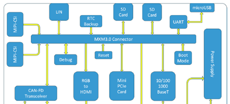
图.评估板SBC-S32V234 CRX-S32V载体板框图
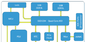
图.评估板SBC-S32V234 MPX-S32V模块框图

图.评估板SBC-S32V234外形图

图评估板SBC-S32V234模块边连接器(载体板CRX-S32V)外形图

图.评估板SBC-S32V234非模块边连接器(载体板CRX-S32V)外形图

图.评估板SBC-S32V234模块(MPX-S32V)外形图(正面)

图.评估板SBC-S32V234模块(MPX-S32V)外形图(背面)
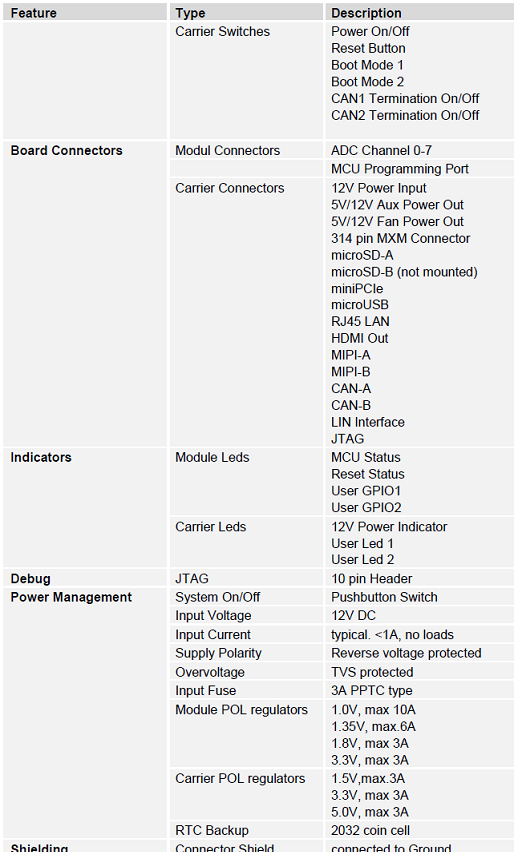
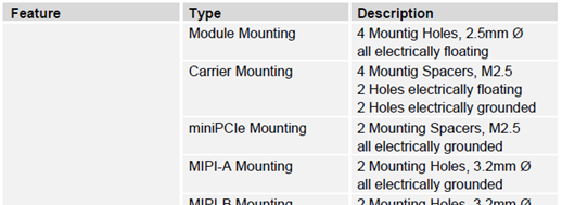
评估板SBC-S32V234主要特性:

详情请见:
责任编辑:Davia
【免责声明】
1、本文内容、数据、图表等来源于网络引用或其他公开资料,版权归属原作者、原发表出处。若版权所有方对本文的引用持有异议,请联系拍明芯城(marketing@iczoom.com),本方将及时处理。
2、本文的引用仅供读者交流学习使用,不涉及商业目的。
3、本文内容仅代表作者观点,拍明芯城不对内容的准确性、可靠性或完整性提供明示或暗示的保证。读者阅读本文后做出的决定或行为,是基于自主意愿和独立判断做出的,请读者明确相关结果。
4、如需转载本方拥有版权的文章,请联系拍明芯城(marketing@iczoom.com)注明“转载原因”。未经允许私自转载拍明芯城将保留追究其法律责任的权利。
拍明芯城拥有对此声明的最终解释权。
相关资讯
:
基于MC33771主控芯片的新能源锂电池管理系统解决方案

AMIC110 32位Sitara ARM MCU开发方案

基于AMIC110多协议可编程工业通信处理器的32位Sitara ARM MCU开发方案

基于展讯SC9820超低成本LTE芯片平台的儿童智能手表解决方案

基于TI公司的AM437x双照相机参考设计

基于MTK6580芯片的W2智能手表解决方案


 2012- 2022 拍明芯城ICZOOM.com 版权所有 客服热线:400-693-8369 (9:00-18:00)


