


 产品分类
产品分类
基于Renesas公司的RX24U 32位MCU马达控制方案
 460
460
 拍明
拍明
原标题:Renesas RX24U 32位MCU马达控制方案
Renesas公司的RX24U是功能强大的内置了差分放大器和安全系统的32位马达控制mcu,工作频率80MHz,集成了浮点单元(FPU),153.6 DMIPS性能,12位ADC,80MHz PWM,512-/384-/256KB代码闪存,8KB数据闪存和32KB SRAM,工作电压2.7V- 5.5V,主要用在通用工业和消费类设备.本文介绍了RX24U主要特性和指标,框图,以及RX24U开发板RSK主要特性和指标,内部框图,元件布局图,调试连接图和电路图.
The RX24U Group features a 32-bit microcontroller ideally suited for dual inverter control with a built-in Floating-Point Unit (FPU) that enables it to easily execute complex inverter control algorithms. The built-in Differential Programmable Gain Amplifier and the provide safety system allow to bring application system cost down.
The easy usability of the RX24U is helping our customers to reduce the time to market by reducing software development efforts and system design by providing a ready-to-go motor control solution, including software and hardware design examples.
RX24U主要特性:
■ 32-bit RXv2 CPU core
• Max.operating frequency:80 MHzCapable of 153.6 DMIPS in operation at 80 MHz
• Enhanced DSP: 32-bit multiply-accumulate and 16-bitmultiply-subtract instructions supported
• Built-in FPU: 32-bit single-precision floating point(compliant to IEEE754)
• Divider (fastest instruction execution takes two CPU clockcycles)
• Fast interrupt
• CISC Harvard architecture with 5-stage pipeline
• Variable-length instructions, ultra-compact code
• On-chip debugging circuit
• Memory protection unit (MPU) supported
■ Low power design and architecture
• Operation from a single 2.7-V to 5.5-V supply
• Three low power consumption modes
■ On-chip code flash memory
• 512-/384-/256-Kbyte capacities
• On-board or off-board user programming
• For instructions and operands
■ On-chip data flash memory
• 8-Kbyte (Number of erase/write cycles: 1,000,000 (typ))
• BGO (Back Ground Operation)
■ On-chip SRAM, no wait states
• 32 Kbytes of SRAM
■ Data transfer functions
• DTC: Four transfer modes
■ Reset and supply management
• Seven types of reset, including the power-on reset (POR)
• Low voltage detection (LVD) with voltage settings
■ Clock functions
• Main clock oscillator frequency: 1 to 20 MHz
• External clock input frequency: Up to 20 MHz
• PLL circuit input: 4 MHz to 12.5 MHz
• On-chip low-speed oscillators, on-chip high-speedoscillators, dedicated on-chip oscillator for the IWDT
• Clock frequency accuracy measurement circuit (CAC)
■ Independent watchdog timer
• 15-kHz on-chip oscillator produces a dedicated clocksignal to drive IWDT operation.
■ Useful functions for IEC60730 compliance
• Self-diagnostic and disconnection-detection assistancefunctions for the A/D converter, clock frequency accuracymeasurement circuit, independent watchdog timer, RAMtest assistance functions using the DOC, etc.
■ MPC
• Multiple locations are selectable for I/O pins of peripheral functions
■ Up to 9 communications channels
• CAN (compliant with ISO11898-1), incorporating 16message boxes (1 channel)
• SCI with many useful functions (6 channels)
Asynchronous mode, clock synchronous mode, smart cardinterface mode, simplified SPI, simplified I2C, andextended serial mode.
• I2C bus interface: Transfer at up to 400 kbps, capable ofSMBus operation (1 channel)
• RSPI capable of high speed connection Transfer at up to 20Mbps (1 channel)
■ Up to 25 extended-function timers
(Up to three-phase complementary PWM3-channel simultaneous output)
• 16-bit MTU3: 80 MHz operation, input capture, outputcompare, three-phase complementary PWM × 2 channelsoutput, CPU-efficient complementary PWM, phase
counting mode (nine channels)
• 16-bit GPT: 80 MHz operation, input capture, outputcompare, PWM wave-form single-phase complementary ×
4 channels output or three-phase complementary ×1 channel + single-phase complementary × 1 channel
output, comparator interlocking operation (Countoperation, PWM negate control) (4 channels)
• 8-bit TMRs (8 channels)
• 16-bit compare-match timers (4 channels)
■ 12-bit A/D converter: 22 channels in 3 units
• Incorporating sample-and-hold circuit 12 bits × 3 units(unit 0: 5 channels, unit 1: 5 channels, unit 2: 12 channels)
• Sampling time can be set for each channel
• Group scan priority control mode (3 levels)
• Self-diagnostic function and analog input disconnectiondetection assistance function (compliant to IEC60730)
• Input signal amplitude by the programmable gain amplifier(4 channels)
• Gain setting reference GND port: 2 ports
• ADC: 3-channel simultaneous sample-and-hold circuit (3shunt method), double data register (1 shunt method),amplifiers (4 channels), comparator (4 channels)
■ 8-bit D/A converter: 2 channels
• This can be used as reference voltage for a comparator
■ Register write protection function can protectvalues in important registers againstoverwriting.
■ Up to 111 pins for general I/O ports
• 5-V tolerant, open drain, input pull-up, switching ofdriving capacity
■ Operating temperature range
• −40 to +85 ℃
RX24U应用:
• General industrial and consumer equipment
RX24U主要指标:


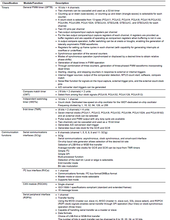

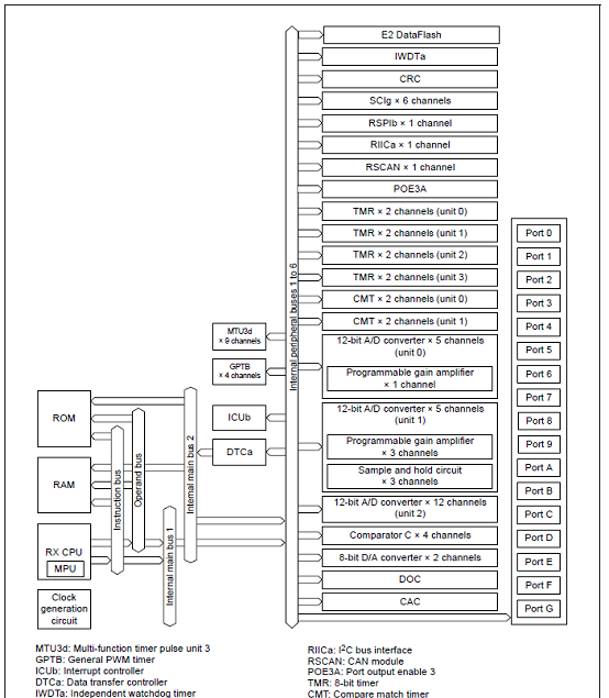
图1.RX24U框图
RX24U开发板RSK
The Renesas Starter Kit for RX24U is the perfect starter kit for developers who are new to the RX24U.
The kit includes an LCD display module, on-chip debugging emulator, and integrated development environment so you can start evaluating the RX24U immediately after opening the box.
Please use this product to experience the performance and functions of the RX24U.
图2.RX24U开发板RSK外形图
RX24U开发板RSK主要特性:
Such as IIC and SCI the communication function can be evaluated.
In addition, CAN can be evaluated.
Including sample codes(Sample programs will be available in Renesas Web site.) Easy to understand coding technique.
Required IBM-PC compatible PC(need USB interface, Processor 1GHz over), OS: Windows 10/8/7/Vista(other than the listed OS is not supported)
RX24U开发板RSK主要指标:
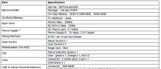
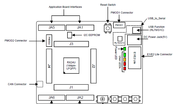
图3.RX24U开发板RSK布局图
责任编辑:Davia
【免责声明】
1、本文内容、数据、图表等来源于网络引用或其他公开资料,版权归属原作者、原发表出处。若版权所有方对本文的引用持有异议,请联系拍明芯城(marketing@iczoom.com),本方将及时处理。
2、本文的引用仅供读者交流学习使用,不涉及商业目的。
3、本文内容仅代表作者观点,拍明芯城不对内容的准确性、可靠性或完整性提供明示或暗示的保证。读者阅读本文后做出的决定或行为,是基于自主意愿和独立判断做出的,请读者明确相关结果。
4、如需转载本方拥有版权的文章,请联系拍明芯城(marketing@iczoom.com)注明“转载原因”。未经允许私自转载拍明芯城将保留追究其法律责任的权利。
拍明芯城拥有对此声明的最终解释权。
相关资讯
:
基于MC33771主控芯片的新能源锂电池管理系统解决方案

AMIC110 32位Sitara ARM MCU开发方案

基于AMIC110多协议可编程工业通信处理器的32位Sitara ARM MCU开发方案

基于展讯SC9820超低成本LTE芯片平台的儿童智能手表解决方案

基于TI公司的AM437x双照相机参考设计

基于MTK6580芯片的W2智能手表解决方案


 2012- 2022 拍明芯城ICZOOM.com 版权所有 客服热线:400-693-8369 (9:00-18:00)


