基于STM32L486JG主控芯片的货道控制板方案
 411
411
 拍明
拍明
应用领域:智能家电
方案类型:模块板卡
主控芯片:STM32L486JG
方案概述
1、项目简介:
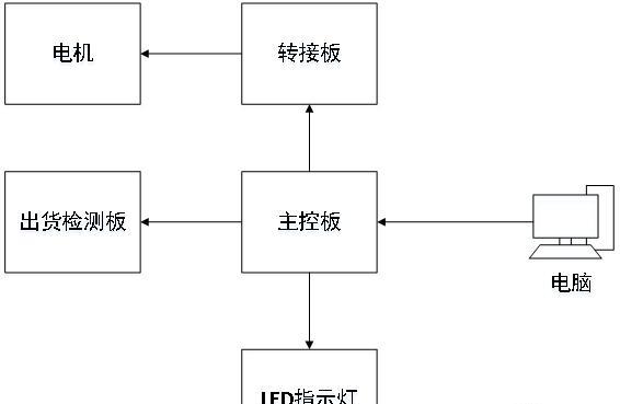
本货道控制板是一套结合软硬件于一体的多层次项目开发,主要是实现通过上位机发送指令控制指定货道电机转动以及出货检测和LED灯的控制等动作。
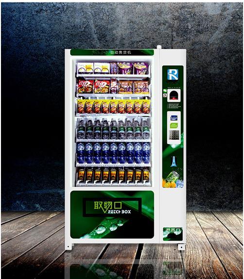
2、项目需求:
1 控制板虚实线短路、过流、过压和欠压等故障保护且控制板需集成货道控制、光电检测、LED等控制等功能;
2 货道控制板通讯检测:上位机通过串口指令发送给货道控制板,货道控制板返回正常或异常;
3 货道控制板检测有无电机、数量:上位机发送检测有无电机指令给货道控制板,货道控制板自检查询货道、电机数量,并返回给上位机;
4 货道测试功能,测试单个或者多个货道是否正常;
5 自动和手动测试光电检测功能;
6 出货控制光电检测及故障反馈功能;
7 集成LED等控制功能;
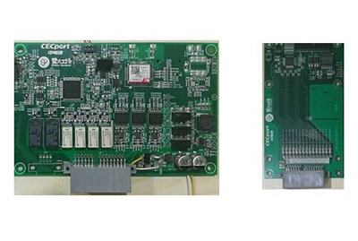
8 采用矩阵排列将所有货道的数据线集合到转接板上便于维护,转接板至少8个以上插口,每个插口控制10 个货道;
9 广电板用于检测商品出货确认,需加大光栅密度且需可调节光栅信号强度。
3、设计框架:
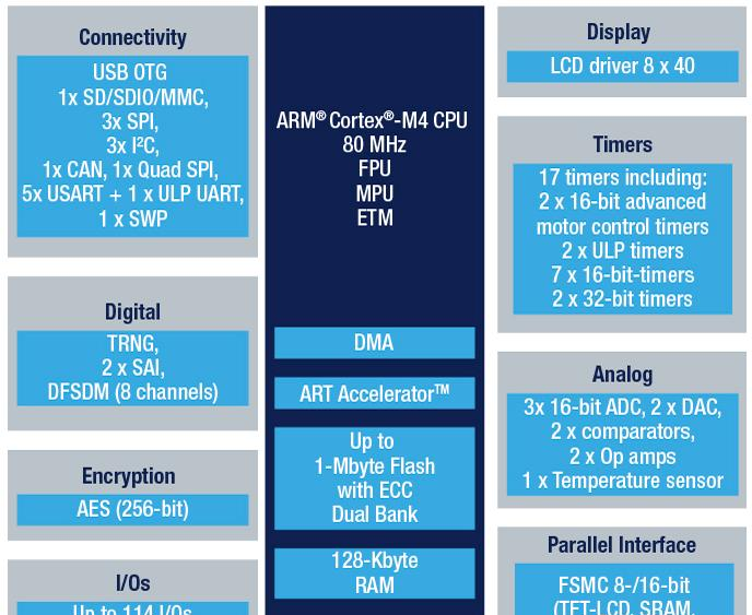
【 STM32L486JG 】
Ultra-low-power with FPU ARM Cortex-M4 MCU 80 MHz with 1 Mbyte Flash, LCD, USB OTG, AES-256, DFSDM
The STM32L486xx devices are the ultra-low-power microcontrollers based on the high-performance ARM® Cortex®-M4 32-bit RISC core operating at a frequency of up to 80 MHz. The Cortex-M4 core features a Floating point unit (FPU) single precision which supports all ARM single-precision data-processing instructions and data types. It also implements a full set of DSP instructions and a memory protection unit (MPU) which enhances application security.
The STM32L486xx devices embed high-speed memories (1 Mbyte of Flash memory, 128 Kbyte of SRAM), a flexible external memory controller (FSMC) for static memories (for devices with packages of 100 pins and more), a Quad SPI flash memories interface (available on all packages) and an extensive range of enhanced I/Os and peripherals connected to two APB buses, two AHB buses and a 32-bit multi-AHB bus matrix.
The STM32L486xx devices embed several protection mechanisms for embedded Flash memory and SRAM: readout protection, write protection, proprietary code readout protection and Firewall.
The devices offer up to three fast 12-bit ADCs (5 Msps), two comparators, two operational amplifiers, two DAC channels, an internal voltage reference buffer, a low-power RTC, two general-purpose 32-bit timer, two 16-bit PWM timers dedicated to motor control, seven general-purpose 16-bit timers, and two 16-bit low-power timers. The devices support four digital filters for external sigma delta modulators (DFSDM).
In addition, up to 24 capacitive sensing channels are available. The devices also embed an integrated LCD driver 8x40 or 4x44, with internal step-up converter.
They also feature standard and advanced communication interfaces.
The STM32L486xx devices embed AES hardware accelerator.
The STM32L486xx operates in the -40 to +85 °C (+105 °C junction), -40 to +105 °C (+125 °C junction) and -40 to +125 °C (+130 °C junction) temperature ranges from a 1.71 to 3.6 V VDD power supply when using internal LDO regulator and a 1.05 to 1.32V VDD12 power supply when using external SMPS supply. A comprehensive set of power-saving modes allows the design of low-power applications.
Some independent power supplies are supported: analog independent supply input for ADC, DAC, OPAMPs and comparators, 3.3 V dedicated supply input for USB and up to 14 I/Os can be supplied independently down to 1.08V. A VBAT input allows to backup the RTC and backup registers. Dedicated VDD12 power supplies can be used to bypass the internal LDO regulator when connected to an external SMPS.
The STM32L486xx family offers five packages from 64-pin to 144-pin packages.
Key Features
Ultra-low-power with FlexPowerControl
1.71 V to 3.6 V power supply
-40 °C to 85/105/125 °C temperature range
300 nA in VBAT mode: supply for RTC and 32x32-bit backup registers
30 nA Shutdown mode (5 wakeup pins)
120 nA Standby mode (5 wakeup pins)
420 nA Standby mode with RTC
1.1 μA Stop 2 mode, 1.4 μA with RTC
100 μA/MHz run mode (LDO Mode)
39 μA/MHz run mode (@3.3 V SMPS Mode)
Batch acquisition mode (BAM)
4 μs wakeup from Stop mode
Brown out reset (BOR)
Interconnect matrix
Core: ARM® 32-bit Cortex®-M4 CPU with FPU, Adaptive real-time accelerator (ART Accelerator™) allowing 0-wait-state execution from Flash memory, frequency up to 80 MHz, MPU, 100DMIPS and DSP instructions
Performance benchmark
1.25 DMIPS/MHz (Drystone 2.1)
273.55 CoreMark® (3.42 CoreMark/MHz @ 80 MHz)
Energy benchmark
220 ULPBENCH® score
Clock Sources
4 to 48 MHz crystal oscillator
32 kHz crystal oscillator for RTC (LSE)
Internal 16 MHz factory-trimmed RC (±1%)
Internal low-power 32 kHz RC (±5%)
Internal multispeed 100 kHz to 48 MHz oscillator, auto-trimmed by LSE (better than ±0.25 % accuracy)
3 PLLs for system clock, USB, audio, ADC
Up to 114 fast I/Os, most 5 V-tolerant, up to 14 I/Os with independent supply down to 1.08 V
RTC with HW calendar, alarms and calibration
LCD 8× 40 or 4× 44 with step-up converter
Up to 24 capacitive sensing channels: support touchkey, linear and rotary touch sensors
16x timers: 2x 16-bit advanced motor-control, 2x 32-bit and 5x 16-bit general purpose, 2x 16-bit basic, 2x low-power 16-bit timers (available in Stop mode), 2x watchdogs, SysTick timer
Memories
1 MB Flash, 2 banks read-while-write, proprietary code readout protection
128 KB of SRAM including 32 KB with hardware parity check
External memory interface for static memories supporting SRAM, PSRAM, NOR and NAND memories
Quad SPI memory interface
4x digital filters for sigma delta modulator
Rich analog peripherals (independent supply)
3× 12-bit ADC 5 Msps, up to 16-bit with hardware oversampling, 200 μA/Msps
2x 12-bit DAC, low-power sample and hold
2x operational amplifiers with built-in PGA
2x ultra-low-power comparators
AES: 128/256-bit key encryption hardware accelerator
20x communication interfaces
USB OTG 2.0 full-speed, LPM and BCD
2x SAIs (serial audio interface)
3x I2C FM+(1 Mbit/s), SMBus/PMBus
5x USARTs (ISO 7816, LIN, IrDA, modem)
1x LPUART (Stop 2 wake-up)
3x SPIs (4x SPIs with the Quad SPI)
CAN (2.0B Active) and SDMMC interface
SWPMI single wire protocol master I/F
IRTIM (Infrared interface)
14-channel DMA controller
True random number generator
CRC calculation unit, 96-bit unique ID
Development support: serial wire debug (SWD), JTAG, Embedded Trace Macrocell™
电路原理图
责任编辑:Davia
【免责声明】
1、本文内容、数据、图表等来源于网络引用或其他公开资料,版权归属原作者、原发表出处。若版权所有方对本文的引用持有异议,请联系拍明芯城(marketing@iczoom.com),本方将及时处理。
2、本文的引用仅供读者交流学习使用,不涉及商业目的。
3、本文内容仅代表作者观点,拍明芯城不对内容的准确性、可靠性或完整性提供明示或暗示的保证。读者阅读本文后做出的决定或行为,是基于自主意愿和独立判断做出的,请读者明确相关结果。
4、如需转载本方拥有版权的文章,请联系拍明芯城(marketing@iczoom.com)注明“转载原因”。未经允许私自转载拍明芯城将保留追究其法律责任的权利。
拍明芯城拥有对此声明的最终解释权。


 产品分类
产品分类




 2012- 2022 拍明芯城ICZOOM.com 版权所有 客服热线:400-693-8369 (9:00-18:00)


