基于MLX90615/R5F100/R5F11AG/EFR32BG1B232/P401N331D主控器件的耳温枪解决方案
 408
408
 拍明
拍明
概述
耳温枪主要由红外温度传感器、主控制器、人机接口、蓝牙无线通讯、电池及电源管理等几大部分组成。要求在35℃到42℃温度范围内,其测量精度在±0.2℃、带LED/LCD显示、语音报警。使用干电池供电超低功耗,同时要求低成本。本方案完全满足以上需求,尤其在精度和功耗方面做得非常突出,也可根据成本和需求选配蓝牙通讯功能。
优势
· MELEXIS红外温度传感器MLX90615,高达0.2℃的医疗级精度,工厂校准。原厂可提供专业支持,降低设计难度,加快产品上市速度。满足国际耳温枪标准,相关客户批量应用,世强常备库存。
【MLX90615】
Melexis推出了可用性极强的MLX90615产品。这是全球第一款整合在超小TO-46封装中的高灵敏红外温度计,而此前TO-46常用于耳式温度计产品。此款性价比极高的超小型非接触式温度计TO-46封装中内置了红外感应器和信号调节芯片,使其能够准确的以数字形式显示测得温度。
MLX90615产品的感应元件是一款带有可感受目标红外辐射的微机械振膜晶片。Melexis的这种技术经过多年工业和汽车温度测量领域中的应用,已经得到了充分的证实。温度计中定制的信号调节芯片能够放大并数字化感应振膜上的热电偶产生的微小电压,同时芯片存储器中储存了工厂设定的刻度参数,能够用来准确的计算目标体的温度。数字形式显示的温度是完全线性的,并且会对环境温度进行补偿。高度的整合性使得MLX90615与过去红外产品相比具有更高的性价比。
MLX90615在信号调节芯片中使用了先进的低噪音放大器,一枚16-bitADC以及功能强大的DSP元件。温度计能适应从-40°C到85°C的广泛工作温度范围,目标的体表可操作温度为-40°C至115°C,测量分辨率保持在0.02°C。MLX90615产品在36°C至39°C的关键温度范围内绝对准确度达到了极高的±0.1°C。
Mlx90615使用3V电源电压,在正常工作中电流的消耗量小于1mA。感应器有节能“睡眠”模式,能够让当前电流消耗量低于2µA。Mlx90615符合AECQ100标准和绿色环保标准RoHS。遵照JEDEC020C它可以在最高260℃温度下焊接。
Melexis红外产品市场经理LucBuydens说:“这款新型智能红外温度计能够让我们的客户更为方便及高效地生产耳式温度计和其他要求高精确度的医用设备。在自我监控和可移动电子装置的应用中,它具有十分理想的功效,其小巧的外形和低功耗特性都具有很高的价值。
特性和益处:
Ø 小尺寸,低成本
Ø 高集成:内部集成了热电堆红外探头+放大+DSP数模转换,
Ø 出厂校准设置宽温度范围(生产过和免校准;节省专业设备,简化生产流程;)
Ø 高(医用)精度:在36°C至39°C的关键温度范围内绝对准确度达到了极高的
Ø SMBus兼容的数字接口;连续读数的客户定制PWM输出
Ø 3V电源电压,省电模式工作能耗仅1 mA
Ø 嵌入式发射率补偿
应用实例:
Ø 高精度非接触温度测量
Ø 手提式温度计
Ø 耳温计
Ø 家用温度控制
Ø 卫生保健
Ø 家畜监控
Ø 多重区域温度控制–可通过公用两线连接100传感器
MLX90615现货供应:
产品型号:
MLX90615SSG-DAG
MLX90615SSG-DAA
MLX90615SSG-DAA-000-TU
MLX90615SSG-DAG-000-TU
封装:TO-46
最少包装:55PCS/管
库存数量:10K
Features and Benefits
Small size, low cost
Easy to integrate
Factory calibrated in wide temperature range: -40…85˚C for sensor temperature and
-40…115˚C for object temperature
High accuracy of 0.5°C over wide temperature
range (0...+50°C for both TA and TO )
High (medical) accuracy
calibration
Measurement resolution of 0.02°C
SMBus compatible digital interface
Power saving mode
Customizable PWM output for continuous
reading
Embedded emissivity compensation
3V supply voltage
Applications Examples
High precision non-contact temperature
measurements
Hand-held thermometers
Ear thermometers
Home appliances with temperature control
Healthcare
Livestock monitoring
Multiple zone temperature control – up to 127
sensors can be read via common 2 wires
· RENESAS RL78系列MCU产品R5F100, R7F0C019 (集成LCD驱动器),内置高速和低速振荡器,无需外置晶振,用IO口来直接驱动LED阵列或LCD驱动器段式LCD显示器,可极大简化外围电路设计,最大化降低系统硬件成本。
【RL78】
RL78 Family
The RL78 Family 16-bit microcontrollers are the convergence of the high CPU performance of the 78K0R and the superb on-chip
functions of the R8C and the 78K, and offer a comprehensive lineup
of 10-128 pin and 1-512 KB products for the 8/16-bit market.
Realizing industry-leading low power consumption at 46 μA/MHz
consumption during normal operation and 0.57 μA/MHz during clock
operation, you can expect greatly improved power efficiency using
RL78 microcontrollers. Built-in features such as a high-precision
(±1%) high-speed on-chip oscillator, background operation data flash capable of 1 million rewrites, temperature sensor, and interface ports for multiple power supplies help reduce system costs and size.
Family Lineup
RL78/G1x
The RL78/G1x (general purpose group) is a true low power MCU series within the RL78 Family.
RL78/L1x
The RL78/L1x microcontroller family is a peripheral rich family of true low power microcontrollers integrating LCD controller/driver, suitable for industrial and consumer LCD display applications. RL78/L1x offer unique display driver functionality to reduce system power consumption.
RL78/H1x
The RL78/H1x microcontroller family is a peripheral rich family of true low power microcontrollers integrating analoig functions, suitable for healthcare applications.
RL78/I1x
The RL78/I1x microcontrollers are part of the RL78 microcontroller family with rich analog integration and support high temperature operation. RL78/I1x is ideal for application specific solutions but also suitable for many general purpose application In the mass market with tough environment operation.
RL78/F1x
The RL78/F1x microcontrollers are suitable for automotive applications. As the successors of both the 78K0R and R8C, they realize low power consumption and are equipped with built-in functions suitable for automotive applications such as CAN communications, advanced timer, and safety functions.
RL78/D1x (Automotive Only)
Renesas is introducing the RL78/D1x as an optimized solution for the BRICs and low-end instrument cluster markets. The RL78/D1x is the successor of 78K0/Dx2 or UPD78082x microcontrollers and suited for car instrument cluster, built-in car instrument cluster dedicated features such as Sound Generator, Stepper Motor Controller/Driver and LCD Segment Controller/Driver etc.
Road Map

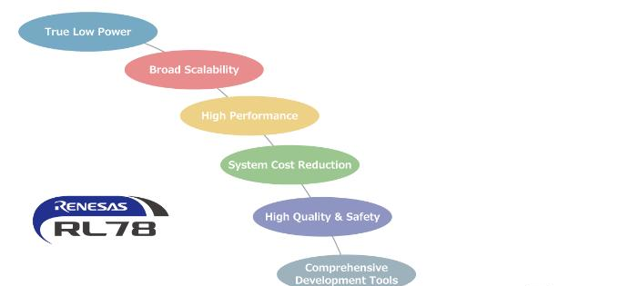
RL78 Family Features
Learn more about the features of the RL78 Family that offer true low power & low voltage operation, high quality & safety, and broad scalability.
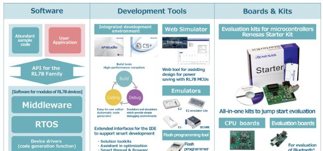
Development Environment for the Renesas RL78 Family MCUs
Renesas Electronics supports all aspects of application development for the RL78 Family with products such as the integrated development environments e² studio and CS+, real-time OSes, and programming tools.
· RENESAS蓝牙SOC R5F11AG系列产品支持蓝牙4.1协议,32个IO可用来直接驱动LED阵列,带低电压检测功能,1.6V到3.6V宽电压供电,低功耗运行和休眠模式可延长电池使用时间。厂家提供各内部模块底层驱动程序、开发板及强大的仿真调试工具。可设计成独立蓝牙模块或者直接替换主控制器。备货充足,高性价比。
【R5F11AG】
RL78/G1D
The RL78/G1D is a microcontroller incorporating the RL78 CPU core and low power consumption RF transceiversupporting the Bluetooth ver.4.2 (Low Energy Single mode) specifications.
1. OUTLINE
1.1 Features
Low Power Technology (3.0V / MCU part: STOP )
• RF transmitter active: 4.3 mA (TYP.)
• RF receiver active: 3.5 mA (TYP.)
• RF sleep (POWER_DOWN mode) operation: 0.3 μA
(TYP.)
On-Chip RF Transceiver
• Bluetooth v4.2 Specification (Low Energy Single mode)
• 2.4 GHz ISM Band, GFSK modulation, TDMA/TDD Frequency Hopping (included AES encryption circuit)
• Adaptivity, exclusively for use in operation as a
slave device
• Single ended RF interface
16-bit RL78-S2 CPU Core
• CISC Architecture (Harvard) with 3-stage pipeline
• Minimum instruction execution time: Can be changed from high speed (0.03125 μs: @ 32 MHz operation with high-speed on-chip oscillator) to ultra-low speed (30.5 μs: @ 32.768 kHz operation with subsystem clock)
• Multiply Signed & Unsigned: 16 x 16 to 32-bit result in
1 clock cycle
• 1-wire on-chip debug function Main Flash Memory
• 128 KB / 192KB / 256 KB (Block size: 1 KB)
• On-chip single voltage flash memory with protection from block erase/writing
• Self-programming with secure boot swap function and flash shield window function Data Flash Memory
• Data Flash with background operation
• Data flash size: 8 KB size (Erase block size: 1 KB)
• Erase Cycles: 1 Million (typ.)
• Erase/programming voltage: 1.8 V to 3.6 V
RAM
• 12 KB / 16KB / 20 KB size
• Supports operands or instructions
• Back-up retention in all modes
On-chip Oscillator
• High accuracy on-chip Oscillator for MCU
• 15kHz low-speed on-chip oscillator for MCU
• 32.768 kHzOn-chip oscillator for the RF slow clock
Data Memory Access (DMA) Controller
• Up to 4 fully programmable channels
• Transfer unit: 8- or 16-bit
Multiple Communication Interfaces
• Simplified I2C×2
• CSI (7-, 8-bit) ×2,
• UART (7-, 8-, 9-bit) ×2
• I2C ×1
Supply voltage Management
• Low voltage detection (LVD) with 12 setting options (Notification to Interrupt and/or reset function)
• Power-on reset (POR) monitor/generator
Extended-Function Timers
• Multi-function 16-bit timers: 8 channels
• Real-time clock (RTC): 1 channel (full calendar and
alarm function with watch correction function)
• Interval Timer: 12-bit, 1 channel
• Watchdog timer: 1 channel (window function)
Rich Analog
• 8/10-bit resolution A/D converter (VDD = 1.6 to 3.6 V)
• Analog input: 8 channels
• Internal voltage reference (1.45 V) and temperature sensorNote Note Can be selected only in HS (high-speed main) mode Safety Functions
• Comply with the IEC60730 and IEC61508 safety standards
General Purpose I/O
• I/O port: 32 (N-ch open drain I/O [withstand voltage of
6 V]: 2, N-ch open drain I/O [VDD withstand voltage]: 9
• Different potential interface support: Can connect to a 1.8/2.5 V device
Standby function
• MCU part: Low power consumption mode: HALT,STOP
Power saving mode: SNOOZE
• RF part :Low power saving mode with 6 setting (min.
0.1 μA)
Operating Voltage / Operating Ambient Temperature
1.6 V to 3.6 V / –40 to +85°C
Package Type and Pin Count
48-pin HWQFN (6 × 6) (0.4mm pitch)
· SILICON LABS蓝牙SOC EFR32BG1B232系列32位ARM Cortex M4内核,主频40MHz,超低功耗。支持2.4GHz蓝牙4.2协议,集成LNA,PA,BALUN等电路,极大简化外围电路设计,集成开发环境功能强大,开发简单,提供评估板。可设计成独立蓝牙模块或者直接替换主控制器。主推型号,备货充足,高性价比。
【EFR32BG】
EFR32BG 2.4 GHz 10.5 dBm Radio Board BRD4100A Reference Manual
The EFR32BG family of Wireless SoCs deliver a high performance,low energy wireless solution integrated into a small form factor package.
By combining a high performance 2.4 GHz RF transceiver with an energy efficient 32-bitMCU, the family provides designers the ultimate in flexibility with a family of pin-compatibledevices that scale from 128/256 kB of flash and 16/32 kB of RAM. The ultra-lowpower operating modes and fast wake-up times of the Silicon Labs energy friendly 32-bit MCUs, combined with the low transmit and receive power consumption of the 2.4 GHz radio, result in a solution optimized for battery powered applications.
To develop and/or evaluate the EFR32 Blue Gecko, the EFR32BG Radio Board can beconnected to the Wireless Starter Kit Mainboard to get access to display, buttons andadditional features from Expansion Boards.

RADIO BOARD FEATURES
• Wireless SoC:EFR32BG1P232F256GM48
• CPU core: ARM Cortex-M4 with FPU
• Flash memory: 256 kB
• RAM: 32 kB
• Operation frequency: 2.4 GHz
• Transmit power: 10.5 dBm
• Integrated PCB antenna, UFL connector(optional).
• Crystals for LFXO and HFXO: 32.768 kHz and 38.4 MHz.
1. Introduction
The EFR32 Blue Gecko Radio Boards provide a development platform (together with the Wireless Starter Kit Mainboard) for the SiliconLabs EFR32 Blue Gecko Wireless System on Chips and serve as reference designs for the matching network of the RF interface.
The BRD4100A Radio Board is designed to operate in the 2400-2483.5 MHz band with the RF matching network optimized to operatewith 10.5 dBm output power.
To develop and/or evaluate the EFR32 Blue Gecko, the BRD4100A Radio Board can be connected to the Wireless Starter Kit Mainboard to get access to display, buttons and additional features from Expansion Boards and also to evaluate the performance of the RFinterface.
2. Radio Board Connector
2.1 Introduction
The board-to-board connector scheme allows access to all EFR32BG1 GPIO pins as well as the RESETn signal. For more information on the functions of the available pin functions, see the EFR32BG1 data sheet.
2.2 Radio Board Connector Pin Associations
The figure below shows the pin mapping on the connector to the radio pins and their function on the Wireless Starter Kit Mainboard.
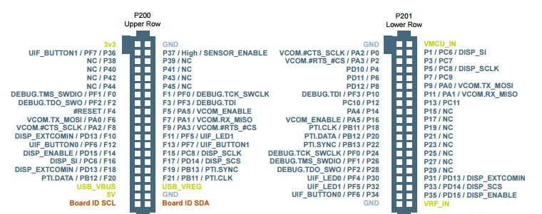
3. Radio Board Block Summary
3.1 Introduction
This section gives a short introduction to the blocks of the BRD4100A Radio Board.
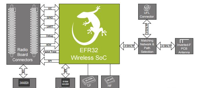
3.2 Radio Board Block Diagram
The block diagram of the EFR32BG Radio Board is shown in the figure below.
3.3 Radio Board Block Description
3.3.1 Wireless MCU
The BRD4100A EFR32 Blue Gecko Radio Board incorporates an EFR32BG1P232F256GM48 Wireless System on Chip featuring 32-bitCortex-M4 with FPU core, 256 kB of flash memory and 32 kB of RAM and a 2.4 GHz band transceiver with output power up to 10.5dBm. For additional information on the EFR32BG1P232F256GM48, refer to the EFR32BG1 Data Sheet.
3.3.2 LF Crystal Oscillator (LFXO)
The BRD4100A Radio Board has a 32.768 kHz crystal mounted.
3.3.3 HF Crystal Oscillator (HFXO)
The BRD4100A Radio Board has a 38.4 MHz crystal mounted.
3.3.4 Matching Network for 2.4 GHz
The BRD4100A Radio Board incorporates a 2.4 GHz matching network which connects the 2.4 GHz TRX pin of the EFR32BG1 to theone on-board printed Inverted-F antenna. The component values were optimized for the 2.4 GHz band RF performace and current consumptionwith 10.5 dBm output power.For detailed description of the matching network, see Chapter 4.2.1 Description of the 2.4 GHz RF Matching.
3.3.5 Inverted-F Antenna
The BRD4100A Radio Board includes a printed Inverted-F antenna (IFA) tuned to have close to 50 Ohm impedance at the 2.4 GHz
band.
For detailed description of the antenna see Chapter 4.5 Inverted-F Antenna.
3.3.6 UFL Connector
To be able to perform conducted measurements, Silicon Labs added an UFL connector to the Radio Board. The connector allows an external 50 Ohm cable or antenna to be connected during design verification or testing.
Note: By default the output of the matching network is connected to the printed Inverted-F antenna by a series component. It can be connected to the UFL connector as well through a series 0 Ohm resistor which is not mounted by default. For conducted measurements through the UFL connector the series component to the antenna should be removed and the 0 Ohm resistor should be mounted (see Chapter 4.2 Schematic of the RF Matching Network for further details).
3.3.7 Radio Board Connectors
Two dual-row, 0.05” pitch polarized connectors make up the EFR32BG Radio
Board interface to the Wireless Starter Kit Mainboard. For more information on
the pin mapping between the EFR32BG1P232F256GM48 and the Radio Board Connector,
refer to Chapter 2.2 Radio Board Connector Pin Associations.
· 理光升压型DC/DC P401N331D,宽输入电压范围0.6V到5.5V,高效率86% (100mA VOUT=3.3V, VIN=1.5V, 25°C),SOT-23-5超小封装。备货充足,高性价比。
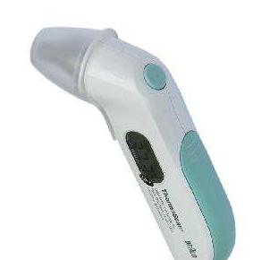
【耳温枪】
耳温枪是属于非接触遥测式(虽然也许还不到一公分)的温度测量仪,它是利用检测鼓膜(相当于下视丘)所发出的红外线光谱来决定体温,根据黑体辐射理论,不同温度的物体所产生的红外线光谱也不同,利用可以精准到0.1℃的温差电堆(Thermopile)红外线侦测器,再以微计算机转换读数而显现出来。
测量原理
红外测温原理
物体处于绝对零度以上时,因为其内部带电粒子的运动,以不同波长的电磁波形式,向外辐射能量,波长涉及紫外、可见、红外光区,但主要处于0.76~3μm的近红外、3~6μm中红外、6~15μm远红外区。物体的红外辐射能量的大小及其按波长的分布与它的表面温度有着十分密切的关系。因此,通过对物体自身辐射的红外能量的测量,便能准确地测定它的表面温度,这就是红外辐射测温所依据的客观。
红外测温仪的工作过程
红外测温仪由光学系统、光电探测器、信号放大器及信号处理、显示输出等部分组成。光学系统汇集其视场内的目标红外辐射能量,视场的大小由测温仪的光学零件以及位置决定。被测物体辐射的红外线首先进入测温仪的光学系统,再由光学系统汇聚射入的红外线,使能量更加集中;聚集后的红外线输入到光电探测器中,探测器的关键部件是红外线传感器,它的任务是把光信号转化为电信号;从光电探测器输出的电信号经过放大器和信号处理电路按照仪器内部的算法和目标发射率校正后转变为被测目标的温度值。
耳温枪的原理
人体鼓膜的辐射能量主要出于6~15μm区。
耳温枪通常使用热电堆传感器,此传感器包含了上述的光学系统、光电探测器---热电堆、热敏电阻。
通过热电堆传感器,检测人体鼓膜的远红外6~15μm的辐射强度。这一测量结果是相对量,即所得结果与被测物的辐射强度和热电堆本身的温度相关。
而热敏电阻则用于测量热电堆本身的温度。
通过计算辐射强度及热电堆本身的温度,即可得到被测物的温度。
责任编辑:Davia
【免责声明】
1、本文内容、数据、图表等来源于网络引用或其他公开资料,版权归属原作者、原发表出处。若版权所有方对本文的引用持有异议,请联系拍明芯城(marketing@iczoom.com),本方将及时处理。
2、本文的引用仅供读者交流学习使用,不涉及商业目的。
3、本文内容仅代表作者观点,拍明芯城不对内容的准确性、可靠性或完整性提供明示或暗示的保证。读者阅读本文后做出的决定或行为,是基于自主意愿和独立判断做出的,请读者明确相关结果。
4、如需转载本方拥有版权的文章,请联系拍明芯城(marketing@iczoom.com)注明“转载原因”。未经允许私自转载拍明芯城将保留追究其法律责任的权利。
拍明芯城拥有对此声明的最终解释权。


 产品分类
产品分类



 2012- 2022 拍明芯城ICZOOM.com 版权所有 客服热线:400-693-8369 (9:00-18:00)


