


 产品分类
产品分类
ST 的SPBTLE-1S是蓝牙Smart v4.2低功耗系统级芯片(SoC)解决方案
 578
578
 拍明
拍明
ST公司的SPBTLE-1S是蓝牙Smart v4.2非常低功耗系统级芯片(SoC)应用处理器模块,基于高性能超低功耗Cortex-M0 32位处理核,嵌入可编程160KB闪存和24KB RAM,和BT标准v4.2和BDE兼容,最大发送功率+ 5 dBm,以微型尺寸集成了无线电,嵌入天线和高频振荡器,提供完整的RF平台.主要用在物联网(IoT),智能家居,建筑物和工业自动化,智能照明,健美和健身与体育,消费类医疗电子,PC和智能手机外设以及安全系统.本文介绍了SPBTLE-1S主要特性和框图,评估板STEVAL-IDB007V1M主要特性和主要元件,电路图,材料清单.
The SPBTLE-1S is a Bluetooth® low Energy System-on-Chip application processor certified module, compliant with BT specifications v4.2 and BQE qualified. The SPBTLE-1S module supports multiple roles simultaneously and can act at the same time as Bluetooth Smart master and slave device.
The SPBTLE-1S is based on BlueNRG-1 system-on-chip and entire Bluetooth Low Energy stack and protocols are embedded into module.
The SPBTLE-1S module provides a complete RF platform in a tiny form factor. Radio, embedded antenna and high frequency oscillators are integrated to offer a certified solution to optimize the time to market of the final applications.
The SPBTLE-1S can be powered directly with a pair of AAA batteries or any power source from 1.7 to 3.6 V.
The SPBTLE-1S is a Bluetooth Low Energy application processor module compliant with Bluetooth® specifications v4.2 with embedded ceramic antenna.
The SPBTLE-1S module has been designed around the ST BlueNRG-1 SoC where its Cortex-M0 core can execute both Bluetooth protocols and customer application. A complete power-optimized Bluetooth stack library provides:
Master, slave, multiple roles support
GAP: central, peripheral, observer or broadcaster roles
Simultaneous advertising and scanning
capability of being slave of up to two masters simultaneously
ATT/GATT: client and server
SM: privacy, authentication and authorization
L2CAP
Link Layer: AES-128 encryption and decryption
The SPBTLE-1S has 160 KB embedded Flash and 24 KB embedded RAM memory.
In the module are available 32 MHz and 32 KHz crystal oscillators. It has been designed to leverage the BlueNRG-1 integrated DC-DC step down converter in order to achieve best power consumption in active mode.
It can be configured to support both application processor (host-less) and network processor (hosted) modes.
Being based on the BlueNRG-1 SoC, the SPBTLE-1S module leverages all the tools and documentation of its ecosystem: Development Kit, Application Notes, User Manuals, Design Notes & Tips. A wide set of sample programs are also available in C source code.
The SPBTLE-1S module has a wide set of peripherals available for customer application (1 x UART interface, 1 x SPI interface, 2 x I2C interface, 14 GPIO, 2 x multifunction timer, 10- bit ADC, Watchdog & RTC, DMA controller, PDM stream processor).
The SPBTLE-1S module enables wireless connectivity into electronic devices, not requiring any RF experience or expertise for integration into the final product. The SPBTLE-1S module provides a complete RF application platform in a tiny form factor (11.5 x 13.5 x 2.0 mm) and being a certified solution optimizes the time to market of the final applications.
The SPBTLE-1S module allows applications to meet the tight advisable peak current requirements imposed with the use of standard coin cell batteries. Optimized results are obtained with the embedded high-efficiency DC-DC step-down. SPBTLE-1S can be powered directly with a standard 3 V coin cell battery as with a pair of AAA batteries or any power source from 1.7 to 3.6 V.
SPBTLE-1S主要特性:
Bluetooth v4.2 compliant
Supports master and slave modes
Multiple roles supported simultaneously
High performance, ultra-low power Cortex-M0 32-bit based architecture core
Programmable embedded 160 KB Flash
24 KB embedded RAM with data retention
Interfaces:
1 x UART, 2 x I²C, 1xSPI, 14 x GPIO, 2 x multifunction timer, 10-bit ADC, Watchdog & RTC, DMA controller, PDM stream processor, SWD debug Interface
Bluetooth radio performance:
Max Tx power: + 5 dBm
Excellent link reliability
On-board chip antenna
Small form factor: 11.5 mm x 13.5 mm
Complemented with Bluetooth low energy protocol stack library (GAP, GATT, SM, L2CAP, LL)
AES security co-processor
Bluetooth low energy SDK with wide range of profile available
Certifications:
EU (RED) Type certificate
SPBTLE-1S应用:
Internet of Things
Smart Home
Building and Industrial Automation
Smart Lighting
Remote and access control
Fitness, wellness and sports
Consumer medical
Security and proximity
Assisted living
PC and smart phone peripherals
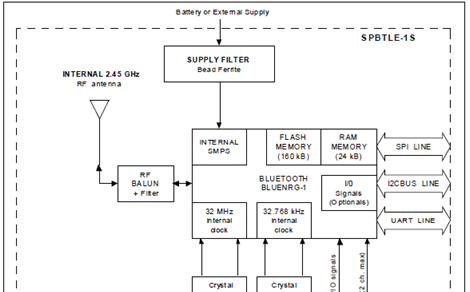
图1.SPBTLE-1S框图
评估板STEVAL-IDB007V1M
The STEVAL-IDB007V1M evaluation platform is based on the SPBTLE-1S, BlueNRG-1 SoC ICs, low power Bluetooth® smart system-on-chip, compliant with the Bluetooth® v4.2 specification and supporting master, slave and simultaneous master-and-slave roles.
The STEVAL-IDB007V1M also provides a set of hardware resources for a wide range of application scenarios: sensor data (accelerometer, pressure and temperature sensors), remote control (buttons and LEDs) and debug message management via USB virtual COM.
Three power options are available (USB only, battery only and external power supply + USB) for high application development and testing flexibility.
评估板STEVAL-IDB007V1M主要特性:
Bluetooth® SMART board with the SPBTLE-1S certified module based on the BlueNRG-1 Bluetooth low energy system-on-chip
Associated BlueNRG-1 development kit SW package including firmware and documentation
Up to +5 dBm available output power
Bluetooth® low energy v4.2 compliant, supports master, slave and simultaneous master-and-slave roles
Integrated balun which integrates a matching network and harmonics filter
SMA connector for antenna or measuring equipment
3 user LEDs
2 user buttons
3D digital accelerometer and 3D digital gyroscope
MEMS pressure sensor with embedded temperature sensor
Battery holder
JTAG debug connector
USB to serial bridge for providing I/O channel with the BlueNRG-1 device
Jumper for measuring current for BlueNRG-1 only
RoHS compliant

图2.评估板STEVAL-IDB007V1M外形图
评估板STEVAL-IDB007V1M包括:
an SPBTLE-1S module development platform
a 2.45 GHz module integrated Bluetooth antenna
a USB cable

图3.评估板STEVAL-IDB007V1M元件图
评估板STEVAL-IDB007V1M元件描述表:


图4.评估板STEVAL-IDB007V1M电路图: Arduino连接器

图5.评估板STEVAL-IDB007V1M电路图:JTAG
")
图6.评估板STEVAL-IDB007V1M电路图: SPBTLE-1S模块(BlueNRG-1)

图7.评估板STEVAL-IDB007V1M电路图:电源管理和传感器

图8.评估板STEVAL-IDB007V1M电路图:按钮和LED

图9.评估板STEVAL-IDB007V1M电路图:微处理器

图10.评估板STEVAL-IDB007V1M电路图:USB,电平转换器, micro JTAG

图11.评估板STEVAL-IDB007V1M电路图:EEPROM/开关
评估板STEVAL-IDB007V1M材料清单:


意法半导体(ST)集团于1988年6月成立,是由意大利的SGS微电子公司和法国Thomson半导体公司合并而成。1998年5月,SGS-THOMSON Microelectronics将公司名称改为意法半导体有限公司。意法半导体是世界最大的半导体公司之一,2006年全年收入98.5亿美元,2007年前半年公司收入46.9亿美元
以业内最广泛的产品组合著称,凭借多元化的技术、尖端的设计能力、知识产权组合、合作伙伴战略和高效的制造能力,意法半导体通过提供创新型半导体解决方案为不同电子应用领域的客户提供服务。[1]
意法半导体(ST)成立于1987年,是意大利SGS微电子公司和法国汤姆逊(Thomson)半导体合并后的新企业。1998年5月,SGS-THOMSON Microelectronics将公司名称改为意法半导体有限公司(STMicroelectronics)。公司自1994年起公开上市,意法半导体股票在纽约证券交易所(交易代码:STM)、泛欧巴黎证券交易所和意大利米兰证券交易所挂牌上市。从成立之初至今,意法半导体的增长速度超过了半导体工业的整体增长速度。自2005年起,意法半导体始终是世界五大半导体公司之一。2006年全年收入98.5亿美元,2007年前半年公司收入46.9亿美元。
整个集团共有员工约50,000人,拥有16个先进的研发机构、39个设计和应用中心、13个主要制造厂,并在36个国家设有78个销售办事处。
公司总部设在瑞士日内瓦,同时也是欧洲、中东和非洲地区(EMEA)市场的总部;公司的美国总部设在德克萨斯州达拉斯市的卡罗顿;亚太区总部设在新加坡;日本的业务则以东京为总部;大中国区总部设在上海,负责香港、大陆和台湾三个地区的业务。
公司销售收入在半导体工业五大高速增长市场之间分布均衡(五大市场占2007年销售收入的百分比):通信(35%),消费(17%),计算机(16%),汽车(16%),工业(16%)。据最新的工业统计数据,意法半导体是全球第五大半导体厂商,在很多市场居世界领先水平。例如,意法半导体是世界第一大专用模拟芯片和电源转换芯片制造商,世界第一大工业半导体和机顶盒芯片供应商,而且在分立器件、手机相机模块和车用集成电路领域居世界前列。
意法半导体(ST)推出一个新的内置闪存的安全型微控制器(MCU),该产品是世界第一个采用90nm (90纳米)制造工艺的微控制器。ST21F384是ST成功的ST21智能卡平台内的第一款安全型微控制器,是为2.5G和3G移动通信优化的产品。新产品改用闪存做程序存储器,淘汰了以前的掩膜ROM,提高了产品制造的灵活性,缩短了从设计到制造的准备时间,同时90nm技术还提高了成本效益。
新的ST21F系列产品使卡制造商能够对飞速变化的手机市场需求做出快速的注重成本效益的反应,然后在制造工序的智能卡个性化阶段自定义应用程序,用一个产品解决多家移动通信网络运营商(MNOs)的要求。因为与一个特定的运营商无关,所以新产品降低了供应链的风险和复杂性。
ST21F384的内核是一个8/16位CPU,线性寻址宽度16MB,典型工作频率21MHz。芯片内置7KB用户RAM存储器,以及128字节页面的384KB闪存,耐擦写能力与早期安全微控制器的EEPROM存储器相当。电流消耗完全符合2G和3G的电源规格,达到了(U)SIM的应用要求。该微控制器含有一个硬件DES (数据加密标准)加速器和用户可以访问的CRC (循环冗余代码)计算模块。
如果采用了这个闪存安全型微控制器,卡制造商将能够缩短在整个制造工序中从设计到投产的准备时间,验证卡上的操作系统(OS)和向运营商提供样片所需的时间会更短。因为可以库存没有编程的空白芯片,所以新产品还有助于缩短产品的量产周期,同时还会大幅度缩短操作功能升级和实现新的MNO要求所需的周期。
由于应用程序保存在闪存内,卡制造商无需再支付ROM掩模成本;此外,因为只需实现最终客户需要的功能,而不必设计一个标准解决方案,应用软件本身可以写得更小。ST的片上闪存装载器提供一个成本低廉的操作系统装载功能。
ST21F384的样片现已上市,定于2007年12月量产。ST的封装能力在业界堪称独一无二,其智能卡IC有两种封装形式:切割过的晶片和先进微型模块,其中模块的集成度和安全性都非常出色。ST21F384产品分为切割过的晶片或没切割过的晶片,模块封装分为6触点(D17)和8触点(D95)两个规格,符合欧洲RoHS环保标准,触点排列符合ISO 7816-2标准。订购100000颗晶片,每颗0.45美元。
详情请见:
![]() en.steval-idb007v1m_schematic.pdf
en.steval-idb007v1m_schematic.pdf
责任编辑:Davia
【免责声明】
1、本文内容、数据、图表等来源于网络引用或其他公开资料,版权归属原作者、原发表出处。若版权所有方对本文的引用持有异议,请联系拍明芯城(marketing@iczoom.com),本方将及时处理。
2、本文的引用仅供读者交流学习使用,不涉及商业目的。
3、本文内容仅代表作者观点,拍明芯城不对内容的准确性、可靠性或完整性提供明示或暗示的保证。读者阅读本文后做出的决定或行为,是基于自主意愿和独立判断做出的,请读者明确相关结果。
4、如需转载本方拥有版权的文章,请联系拍明芯城(marketing@iczoom.com)注明“转载原因”。未经允许私自转载拍明芯城将保留追究其法律责任的权利。
拍明芯城拥有对此声明的最终解释权。
相关资讯
:
基于MC33771主控芯片的新能源锂电池管理系统解决方案

AMIC110 32位Sitara ARM MCU开发方案

基于AMIC110多协议可编程工业通信处理器的32位Sitara ARM MCU开发方案

基于展讯SC9820超低成本LTE芯片平台的儿童智能手表解决方案

基于TI公司的AM437x双照相机参考设计

基于MTK6580芯片的W2智能手表解决方案


 2012- 2022 拍明芯城ICZOOM.com 版权所有 客服热线:400-693-8369 (9:00-18:00)


