Renesas RX72N 240MHz 32位RX MCU开发方案
 102
102
 拍明
拍明
原标题:Renesas RX72N 240MHz 32位RX MCU开发方案
Renesas公司的RX72N是240MHz 32位RX mcu,具有片上双精度64位 IEEE-754 FPU和1396 CoreMark,用于三角函數的运算单元,多达4MB闪存,1MB SRAM,以及各种通信接口,包括和IEEE 1588兼容的以太网MAC,SD主接口,四SPI和CAN.此外还包括了12位ADC和DAC,RTC,加密功能(可选),串行声接口,CMOS照相机接口,图像LCD控制器以及2D绘图引擎.工作电压2.7到 3.6-V,工作温度-40度C到85度C和-40度C到105度C.主要用在消费类电子和工业应用.中电网为您整理如下详细资料,本文介绍了RX72N MCU主要特性, MCU框图以及RX72N 评估板RTK5RX72N0C00000BJ主要特性,框图,电路图和材料清单.
The RX72N Group microcontrollers are equipped with the third-generation RX CPU core, the RXv3 core, and these high-performance products operate at 240MHz. Real-time control and networking of equipment are realized with a single chip with 4MB flash memory capable of read operations at 120MHz, 1MB of SRAM and 182 general-purpose I/O ports. The device also supports high-end HMI functionality for advanced display capability. The device also has complete security capability, vital for industrial and consumer equipment today. The RX72N can also contribute to the miniaturization of the housing and the shortening of the development cycle.
RX72N MCU主要特性:
■ 32-bit RXv3 CPU core
Maximum operating frequency: 240 MHz
Capable of 1396 CoreMark in operation at 240 MHz
Double-precision 64-bit IEEE-754 floating point
A collective register bank save function is available.
Supports the memory protection unit (MPU)
JTAG and FINE (one-line) debugging interfaces
■ Low-power design and architecture
Operation from a single 2.7- to 3.6-V supply
RTC is capable of operation from a dedicated power supply.
Four low-power modes
■ On-chip code flash memory
Supports versions with up to 4 Mbytes of ROM
No wait cycles at up to 120 MHz or when the ROM cache is hit, one-wait state at above 120 MHz
User code is programmable by on-board or off-board programming.
Programming/erasing as background operations (BGOs)
A dual-bank structure allows exchanging the start-up bank.
■ On-chip data flash memory
32 Kbytes, reprogrammable up to 100,000 times
Programming/erasing as background operations (BGOs)
■ On-chip SRAM
1 Mbyte of SRAM (no wait states; however, if ICLK is at a frequency above 120 MHz, access to locations in the 512 Kbytes of SRAM from 0080 0000h to 0087 FFFFh requires one cycle of waiting)
32 Kbytes of RAM with ECC (single error correction/double error detection)
8 Kbytes of standby RAM (backup on deep software standby)
■ Data transfer
DMACAa: 8 channels
DTCb: 1 channel
EXDMAC: 2 channels
DMAC for the Ethernet controller: 3 channels
■ Reset and supply management
Power-on reset (POR)
Low voltage detection (LVD) with voltage settings
■ Clock functions
External crystal resonator or internal PLL for operation at 8 to 24
MHz
PLL for specific purposes
Internal 240-kHz LOCO and HOCO selectable from 16, 18, and 20 MHz
120-kHz clock for the IWDTa
■ Real-time clock
Adjustment functions (30 seconds, leap year, and error)
Real-time clock counting and binary counting modes are selectable
Time capture function (for capturing times in response to event-signal input)
■ Independent watchdog timer
120-kHz clock operation
■ Useful functions for IEC60730 compliance
Oscillation-stoppage detection, frequency measurement, CRCA, IWDTa, self-diagnostic function for the A/D converter, etc.
Register write protection function can protect values in important
registers against overwriting.
■ Various communications interfaces
Ethernet MAC compliant with IEEE 1588 (2 channels)
PHY layer (1 channel) for host/function or OTG controller (1 channel) with full-speed USB 2.0 transfer
CAN (compliant with ISO11898-1), incorporating 32 mailboxes (up to 3 channels)
SCIj and SCIh with multiple functionalities (up to 8 channels)
Choose from among asynchronous mode, clock-synchronous mode, smart-card interface mode, simplified SPI, simplified I2C, and extended serial mode.
SCIi with 16-byte transmission and reception FIFOs (up to 5 channels)
I2C bus interface for transfer at up to 1 Mbps (3 channels)
Four-wire QSPI (1 channel) in addition to RSPIc (3 channels)
Parallel data capture unit (PDC) for the CMOS camera interface (except for 100-pin products)
Graphic-LCD controller (GLCDC)
2D drawing engine (DRW2D)
SD host interface (1 channel) with a 1- or 4-bit SD bus for use with SD memory or SDIO
MMCIF with 1-, 4-, or 8-bit transfer bus width
■ External address space
Buses for full-speed data transfer (max. operating frequency of 80 MHz)
8 CS areas
8-, 16-, or 32-bit bus space is selectable per area
Independent SDRAM area (128 Mbytes)
■ Up to 29 extended-function timers
32-bit GPTW (4 channels)
16-bit TPUa (6 channels), MTU3a (9 channels)
8-bit TMRa (4 channels), 16-bit CMT (4 channels), 32-bit CMTW (2 channels)
■ 12-bit A/D converter
Two 12-bit units (8 channels for unit 0; 21 channels for unit 1)
Self diagnosis, detection of analog input disconnection
■ 12-bit D/A converter: 2 channels
■ Temperature sensor for measuring temperature within the chip
■ Arithmetic unit for trigonometric functions
■ Encryption functions (optional)
AES (key lengths: 128, 192, and 256 bits)
Trusted Secure IP (TSIP)
■ Up to 182 pins for general I/O ports
5-V tolerance, open drain, input pull-up, switchable driving ability
■ Operating temp. range
D-version: –40C to +85C
G-version: –40C to +105C
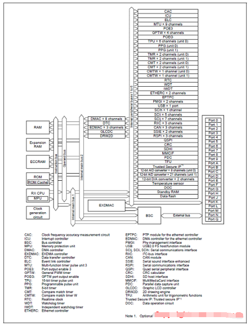
图1. RX72N MCU框图
RX72N 评估板RTK5RX72N0C00000BJ
Thank you for purchasing the RX72N Envision Kit evaluation tool from Renesas (the product). The contents of the product package are as follows:
RX72N Envision Kit (RTK5RX72N0C00000BJ)
The product is an evaluation tool for Renesas MCUs. This manual describes the technical elements of the product’s hardware.
评估板RTK5RX72N0C00000BJ 主要特性:
• Simplified evaluation and development using RX72N MCU
• Support for new functions of the RX72N: LCD controller, 2D rendering engine, dual-bank flash memory, etc.
• Encryption key management functions of Trusted Secure IP, which incorporates encryption accelerators for multiple encryption standards
• 4.3-inch WQVGA TFT panel with capacitive touch functionality
• Wi-Fi/BLE, Ethernet, and USB interfaces
• SD card, on-board memory, and USB Host storage class as standard storage options
• Sound interface and light sensor
• On-board emulator circuit
• Sample application including firmware update function
评估板RTK5RX72N0C00000BJ主要指标:

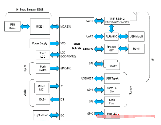
图2. 评估板RTK5RX72N0C00000BJ框图
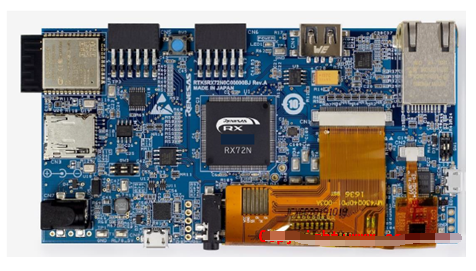
图3. 评估板RTK5RX72N0C00000BJ外形图(元件面)
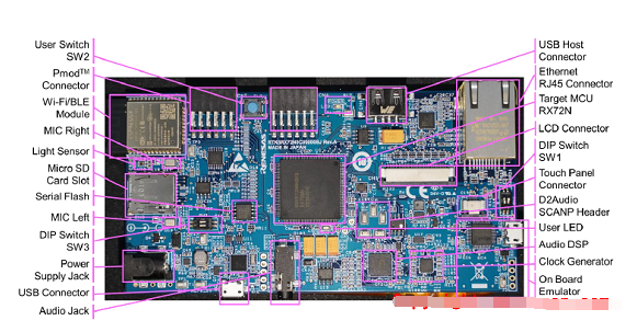
图4. 评估板RTK5RX72N0C00000BJ外形图(元件功能面)不包括LCD
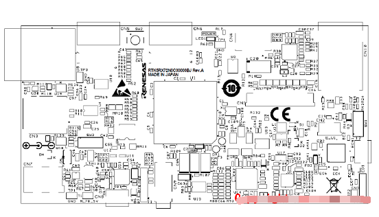
图5. 评估板RTK5RX72N0C00000BJ外形图(元件布局面)
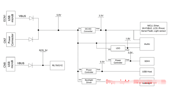
图6. 评估板RTK5RX72N0C00000BJ电源系统框图
责任编辑:David
【免责声明】
1、本文内容、数据、图表等来源于网络引用或其他公开资料,版权归属原作者、原发表出处。若版权所有方对本文的引用持有异议,请联系拍明芯城(marketing@iczoom.com),本方将及时处理。
2、本文的引用仅供读者交流学习使用,不涉及商业目的。
3、本文内容仅代表作者观点,拍明芯城不对内容的准确性、可靠性或完整性提供明示或暗示的保证。读者阅读本文后做出的决定或行为,是基于自主意愿和独立判断做出的,请读者明确相关结果。
4、如需转载本方拥有版权的文章,请联系拍明芯城(marketing@iczoom.com)注明“转载原因”。未经允许私自转载拍明芯城将保留追究其法律责任的权利。
拍明芯城拥有对此声明的最终解释权。


 产品分类
产品分类




 2012- 2022 拍明芯城ICZOOM.com 版权所有 客服热线:400-693-8369 (9:00-18:00)


