Renesas ISL78083汽车照相机电源管理方案
 150
150
 拍明
拍明
原标题:Renesas ISL78083汽车照相机电源管理方案
Renesas公司的ISL78083是汽车照相机电源管理集成电路,具有三个同步降压稳压器和一个低压降线性稳压器.ISL78083是多轨电源器件,包含了一个基本的高压同步降压稳压器,两个低压同步降压稳压器和一个LDO稳压器.器件还提供四个过压和欠压监视器,三个功率良好指示器和重置输出/故障指示器.为了限制共同原因故障,器件还包括用于OV/UV监视器的第二个基准,独立于稳压器的基准.VIN工作电压从4.0V到42V,起动范围从4.5V到42V,固定开关频率2.2MHz.ISL78083采用4mmx4mm 24 Ld Step Cut QFN (SCQFN)封装,满足AEC-Q100规范Grade 1,工作温度-40℃ 到125℃,结温在-40℃ 到150℃.主要用在后视图和环绕视图HD汽车照相机,驾驶员监视照相机和HD行车记录仪.本文介绍了ISL78083主要特性,框图,典型应用电路图和评估板ISL78083DEMO1Z主要特性,主要指标和框图,电路图,材料清单和PCB设计图.
Automotive Camera Power Management IC with Three Synchronous Buck Regulators
and One Low Dropout Linear Regulator
The ISL78083 is a versatile multi-rail power IC comprised of a primary high voltage synchronous buck regulator, two secondary low voltage synchronous buck regulators, and an LDO regulator.
It also offers four overvoltage and undervoltage monitors, three power-good indicators, and a reset output/fault indicator. To limit common-cause failures, the ISL78083 also includes a second reference for the OV/UV monitors, independent from the reference of
the regulators.
The ISL78083 is intended for high-density power applications, requiring few external components and minimal board space. It offers an extensive feature set configured using internal One-Time Programmable (OTP) memory. Nearly all device options, such as each output voltage selection, power sequencing, and OV/UV thresholds are internally configured and require no external components for selection. The regulators also offer internal compensation. The bucks are synchronous to achieve high efficiency and are capable of operating in harsh environments requiring high ambient temperature.
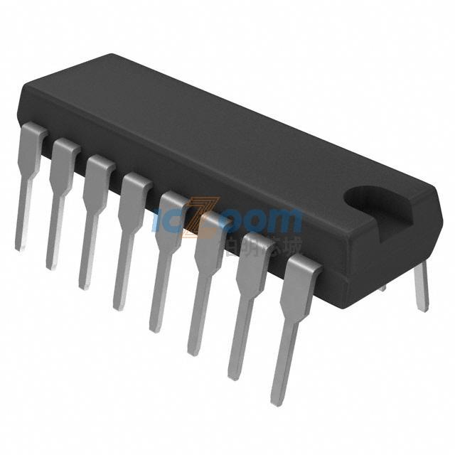
ISL78083 is available in a 4mmx4mm 24 Ld Step Cut QFN (SCQFN) package with an exposed pad for improved thermal performance. It is AEC-Q100 qualified to Grade 1 and operates across an ambient temperature range of -40℃ to 125℃ and is electrically specified across a junction temperature range of -40℃ to 150℃.
ISL78083主要特性:
• VIN operating range from 4.0V to 42V
○ Start range: 4.5V to 42V
• Fixed switching frequency: 2.2MHz with optional pseudo-random spread spectrum
• Three synchronous bucks with internal compensation and one LDO
○ Buck1 output range: 3.3V to 5.05V
○ Buck2 output range: 1.0V to 3.3V
○ Buck3 output range: 1.0V to 3.3V
○ LDO4 output range: 2.8V to 3.4V
• Output UV/OV thresholds, OTP: ±4%, ±6%, ±8%, ±12%
• OTP power up/down sequence and delay
• Optional output discharge on Buck2, Buck3, and LDO4
• Current at VIN input under shutdown: <1μA typical
• Protection features
○ Input voltage UVLO
○ Output OV/UV
○ Positive and negative current limits on bucks
○ Overcurrent protection on internal and output LDOs
○ Fail-safe controller
○ CRC of OTP registers
○ OTP hiccup or latch-off fault response
ISL78083应用:
• Rear and surround view HD automotive cameras
• Driver monitoring cameras
• HD dash cam

图.ISL78083框图

图.ISL78083典型应用电路图
评估板ISL78083DEMO1Z
The ISL78083DEMO1Z demonstrates the performance of the ISL78083 multi-output DC/DC regulator comprised of a primary high voltage buck regulator, two secondary low voltage synchronous buck regulators, and a secondary low voltage LDO regulator. The ISL78083 is intended for high-density power applications, requiring few external components and minimal board space. The ISL78083 provides up to four regulated outputs with full protection and offers three power-good indicators and a reset/fault indicator.
评估板ISL78083DEMO1Z主要特性:
• VIN operating range from 4.0V to 42V
○ Start range: 4.5V to 42V
• Fixed switching frequency: 2.2MHz with optional pseudo-random spread spectrum
• Three synchronous bucks with internal compensation and one LDO
○ Buck1 output range: 3.3V to 5.05V
○ Buck2 output range: 1.0V to 3.3V
○ Buck3 output range: 1.0V to 3.3V
○ LDO4 output range: 2.8V to 3.4V
• Output UV/OV thresholds, OTP: ±4%, ±6%, ±8%, ±12%
• OTP power up/down sequence and delay
• Optional output discharge on Buck2, Buck3, and LDO4
• Current at VIN input under shutdown: <1μA typical
• Protection features
○ Input voltage UVLO
○ Output OV/UV
○ Positive and negative current limits on bucks
○ Overcurrent protection on internal and output LDOs
○ Fail-safe controller
○ CRC of OTP registers
• OTP hiccup or latch-off fault response
评估板ISL78083DEMO1Z主要指标:
• VIN = 4V to 42V (start range: 4.5V to 42V)
• Buck1 output range: 3.3V to 5.05V, up to 0.75A
• Buck2 output range: 1.0V to 3.3V, up to 0.75A
• Buck3 output range: 1.0V to 3.3V, up to 0.75A
• LDO4 output range: 2.8V to 3.4V, up to 0.3A
• Three power-good indicators
• Reset output/fault indicator

图.评估板ISL78083DEMO1Z框图

图.评估板ISL78083DEMO1Z外形连接图
评估板ISL78083DEMO1Z材料清单:


图.评估板ISL78083DEMO1Z外形图(顶面)

图.评估板ISL78083DEMO1Z外形图(底面)

图8.评估板ISL78083DEMO1Z PCB设计图(顶层装配)
责任编辑:David
【免责声明】
1、本文内容、数据、图表等来源于网络引用或其他公开资料,版权归属原作者、原发表出处。若版权所有方对本文的引用持有异议,请联系拍明芯城(marketing@iczoom.com),本方将及时处理。
2、本文的引用仅供读者交流学习使用,不涉及商业目的。
3、本文内容仅代表作者观点,拍明芯城不对内容的准确性、可靠性或完整性提供明示或暗示的保证。读者阅读本文后做出的决定或行为,是基于自主意愿和独立判断做出的,请读者明确相关结果。
4、如需转载本方拥有版权的文章,请联系拍明芯城(marketing@iczoom.com)注明“转载原因”。未经允许私自转载拍明芯城将保留追究其法律责任的权利。
拍明芯城拥有对此声明的最终解释权。


 产品分类
产品分类



 2012- 2022 拍明芯城ICZOOM.com 版权所有 客服热线:400-693-8369 (9:00-18:00)


