


 产品分类
产品分类
ST STM32WB50CG多协议无线ARM MCU开发应用方案
 194
194
 拍明
拍明
原标题:ST STM32WB50CG多协议无线ARM MCU开发应用方案
ST公司的STM32WB50CG是多协议无线和超低功耗MCU,嵌入了功能强大与超低功耗和Bluetooth®低功耗SIG指标v5.0或IEEE 802.15.4-2011兼容的无线电.器件包含了专用的Arm® Cortex® -M0+,以实现所有实时低层运营. STM32WB50CG具有极低的功耗,并基于高性能Arm® Cortex®-M4 32位RISC核,工作频率高达64MHz. Arm® Cortex®-M4核具有浮点单元(FPU)单精度,支持所有的ARM单精度数据处理指令和数据类型,还能实现全套DSP指令,和增强应用安全性的存储器保护单元(MPU).增强的内部处理器通信由六个双向通路的IPCC提供.HSEM提供硬件信号量,用来两个处理器间共享共通资源. STM32WB50CG嵌入一个低功耗RTC,一个先进的16位计时器,一个通用32位计时器,两个通用16位计时器和两个16位低功耗计时器.此外还有标准和先进的通信接口如 一个USART(ISO 7816, IrDA, Modbus和智能卡模式),一个I2C(SMBus/PMBus),一个SPI(高达32MHz).工作电压2-3.6V,工作温度-10 到 +85 °C (+105 °C 结温).主要用在远程传感器,可穿戴跟踪器,楼宇自动化控制器,计算机外围设备,四轴飞行器和其它物联网设备.本文介绍了STM32WB50CG主要特性,框图, RF前端框图,时钟树图,电源方案图以及评估板Nucleo包(P-NUCLEO-WB55)包括Nucleo-68板和USB dongle板的主要特性和电路图.
The STM32WB50CG multiprotocol wireless and ultra-low-power device embeds a powerful and ultra-low-power radio compliant with the Bluetooth® Low Energy SIG specification v5.0 or with IEEE 802.15.4-2011. They contain a dedicated Arm® Cortex® -M0+ for performing all the real-time low layer operation.
The STM32WB50CG device is designed to be extremely low-power and are based on the high-performance Arm® Cortex®-M4 32-bit RISC core operating at a frequency of up to 64 MHz. The Cortex®-M4 core features a Floating point unit (FPU) single precision that supports all Arm® single-precision data-processing instructions and data types. It also implements a full set of DSP instructions and a memory protection unit (MPU) that enhances application security.
Enhanced inter-processor communication is provided by the IPCC with six bidirectional channels. The HSEM provides hardware semaphores used to share common resources between the two processors.
The STM32WB50CG device embeds high-speed memories (Flash memory 1 Mbyte, up to 128 Kbyte of SRAM) and an extensive range of enhanced I/Os and peripherals.
Direct data transfer between memory and peripherals and from memory to memory is supported by seven DMA channels with a full flexible channel mapping by the DMAMUX peripheral.
The STM32WB50CG device embeds several mechanisms for embedded Flash memory and SRAM: readout protection, write protection and proprietary code readout protection. Portions of the memory can be secured for Cortex® -M0+ exclusive access.
The AES encryption engine, PKA and RNG enable lower layer MAC and upper layer cryptography. A customer key storage feature may be used to keep the keys hidden.
The device offers one fast 16-bit ADC.
The STM32WB50CG device embeds a low-power RTC, one advanced 16-bit timer, one general-purpose 32-bit timer, two general-purpose 16-bit timers, and two 16-bit low-power timers.
They also feature standard and advanced communication interfaces:
• one USART (ISO 7816, IrDA, Modbus and Smartcard mode)
• one I2C (SMBus/PMBus)
• one SPI (up to 32 MHz)
The STM32WB50CG operates in the -10 to +85 °C (+105 °C junction) temperature range from a 2 to 3.6 V power supply. A comprehensive set of power-saving modes enables the design of low-power applications.
The STM32WB50CG includes independent power supplies for analog input for ADC.
A VBAT dedicated supply allows the device to back up the LSE 32.768KHz oscillator, the RTC and the backup registers, thus enabling the STM32WB50CG to supply these functions even if the main VDD is not present through a CR2032-like battery, a Supercap or a small rechargeable battery.
The STM32WB50CG is available in a 48-pin UFQFPN package
STM32WB50CG主要特性:
• Includes ST state-of-the-art patented technology
• Radio
– 2.4 GHz
– RF transceiver supporting Bluetooth® 5 specification or IEEE 802.15.4-2011 PHY and MAC, supporting Thread and ZigBee® 3.0
– RX Sensitivity: -96 dBm (Bluetooth® Low Energy at 1 Mbps), -100 dBm (802.15.4)
– Programmable output power up to +4 dBm with 1 dB steps – Integrated balun to reduce BOM
– Support for 1 Mbps – Dedicated Arm® 32-bit Cortex® M0 + CPU for real-time Radio layer
– Accurate RSSI to enable power control
– Suitable for systems requiring compliance with radio frequency regulations ETSI EN 300 328, EN 300 440, FCC CFR47 Part 15 and ARIB STD-T66
– Support for external PA
– Available integrated passive device (IPD) companion chip for optimized matching solution MLPF-WB55-01E3
• Ultra-low-power platform
– 2 V to 3.6 V power supply
– – 10 °C to +85 °C temperature range
– 14 nA shutdown mode
– 700 nA Standby mode + RTC + 32 KB RAM
– 2.25 μA Stop mode + RTC + 128 KB RAM
– Radio: Rx 7.9 mA / Tx at 0 dBm 12 mA
• Core: Arm® 32-bit Cortex®-M4 CPU with FPU, adaptive real-time accelerator (ART Accelerator™) allowing 0-wait-state execution from Flash memory, frequency up to 64 MHz, MPU, 80 DMIPS and DSP instructions
• Performance benchmark
– 1.25 DMIPS/MHZ(Drystone 2.1)
– 219.48 Coremark® (3.43 Coremark/MHz @64 MHz)
• Energy benckmark
– 303 ULPMark™ CP score
• Supply and reset management
– Ultra-safe, low-power BOR (brownout reset) with five selectable thresholds
– Ultra-low-power POR/PDR
– Programmable voltage detector (PVD)
– VBAT mode with RTC and backup registers
• Clock sources
– 32 MHz crystal oscillator with integrated trimming capacitors (Radio and CPU clock)
– 32 kHz crystal oscillator for RTC (LSE)
– Internal low-power 32 kHz (±5%) RC (LSI1)
– Internal low-power 32 kHz (stability ±500 ppm) RC (LSI2)
– Internal multispeed 100 kHz to 48 MHz oscillator, auto-trimmed by LSE (better than ±0.25% accuracy) – High speed internal 16 MHz factory trimmed RC (±1%)
– 1x PLL for system clock and ADC
• Memories
– 1 MB Flash memory with sector protection (PCROP) against R/W operations, enabling authentic Bluetooth® Low Energy and 802.15.4 SW stack
– 128 KB SRAM, including 64 KB with hardware parity check
– 20x32-bit backup register
– Boot loader supporting, USART, SPI, I2C
– OTA (Over the air) Bluetooth® Low Energy and 802.15.4 update
• Rich analog peripherals (down to 2 V)
– 12-bit ADC 2.13 Msps, up to 16-bit with hardware oversampling, 200 μA/Msps
• System peripherals
– Inter processor communication controller (IPCC) for communication with Bluetooth® Low Energy and 802.15.4
– HW semaphores for resources sharing between CPUs
– 1x DMA controllers (7x channels) supporting ADC, SPI, I2C, USART, AES, Timers
– 1x USART (ISO 7816, IrDA, SPI Master, Modbus and Smartcard mode)
– 1x SPI 32 Mbit/s
– 1x I2C (SMBus/PMBus)
– 1x 16-bit, four channels advanced timer
– 2x 16-bits, two channels timer
– 1x 32-bits, four channels timer
– 2x 16-bits ultra-low-power timer
– 1x independent Systick
– 1x independent watchdog
– 1x window watchdog
• Security and ID
– Secure firmware installation (SFI) for Bluetooth® Low Energy and 802.15.4 SW stack
– 2x hardware encryption AES maximum 256-bit for the application, the Bluetooth® Low Energy and IEEE802.15.4
– Customer key storage / key manager services
– HW public key authority (PKA)
– Cryptographic algorithms: RSA, Diffie-Helman, ECC over GF(p)
– True random number generator (RNG)
– Sector protection against R/W operation (PCROP)
– CRC calculation unit
– Die information: 96-bit unique ID
– IEEE 64-bit unique ID. Possibility to derive 802.15.4 64-bit and Bluetooth® Low Energy 48-bit EUI
• Up to 30 fast I/Os, 28 of them 5 V-tolerant
• Development support
– Serial wire debug (SWD), JTAG for the Application processor
– Application cross trigger
• All packages are ECOPACK®2 compliant
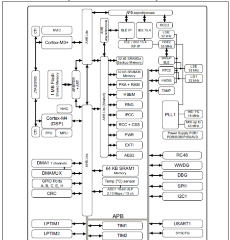
图1. STM32WB50CG框图
Architecture
The STM32WB50CG multiprotocol wireless device embeds a BLE or an 802.15.4 RF subsystem that interfaces with a generic microcontroller subsystem using an Arm® Cortex®-M4 CPU (called CPU1) on which the host application resides.
The RF subsystem is composed of a RF Analog Front end, BLE or 802.15.4 digital MAC blocks as well as of a dedicated Arm® Cortex®-M0+ microcontroller (called CPU2) plus some proprietary peripherals. The RF subsystem performs all of the BLE or 802.15.4 low layer stack, reducing the interaction with the CPU1 to high level exchanges.
Some functions are shared between the RF subsystem CPU (CPU2) and the Host CPU (CPU1):
The communication and the sharing of peripherals between the RF subsystem and the Cortex®-M4 CPU is performed through a dedicated Inter Processor Communication Controller (IPCC) and semaphore mechanism (HSEM).
• Flash memories
• SRAM1, SRAM2a and SRAM2b (SRAM2a can be retained in Standby mode)
• Security peripherals (RNG, PKA)
• Clock RCC
• Power control (PWR)
Arm® Cortex®-M4 core with FPU
The Arm® Cortex®-M4 with FPU processor is a processor for embedded systems. It has been developed to provide a low-cost platform that meets the needs of MCU implementation, with a reduced pin count and low-power consumption, while delivering outstanding computational performance and an advanced response to interrupts.
The Arm® Cortex®-M4 with FPU 32-bit RISC processor features exceptional code-efficiency, delivering the high-performance expected from an Arm® core in the memory size usually associated with 8- and 16-bit devices.
The processor supports a set of DSP instructions which allow efficient signal processing and complex algorithm execution.
Its single precision FPU speeds up software development by using metalanguage development tools, while avoiding saturation.
With its embedded Arm® core, the STM32WB50CG is compatible with all Arm® tools and software.
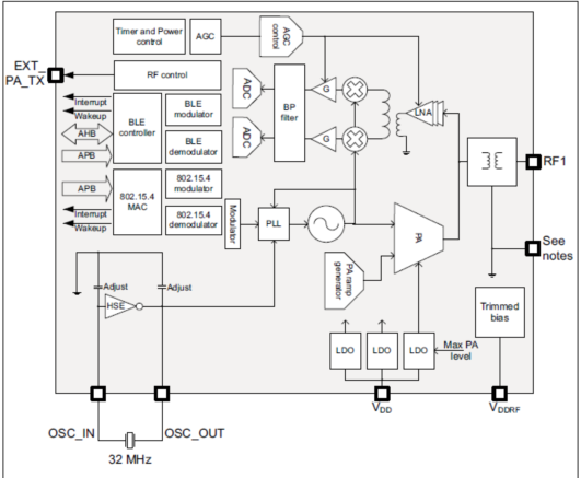
图2. STM32WB50CG RF前端框图
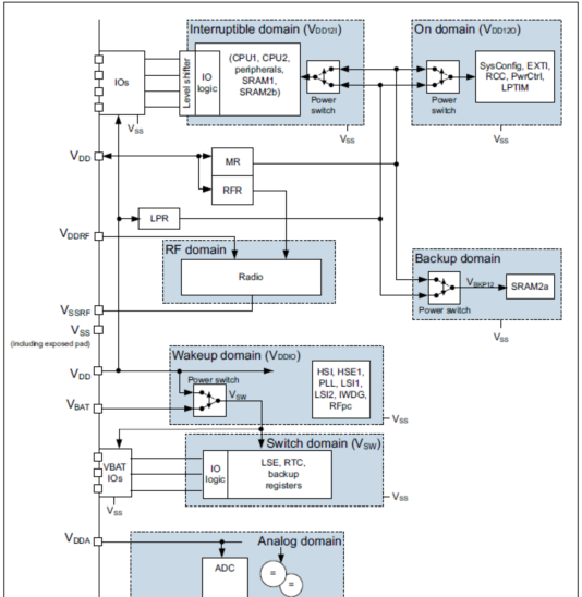
图3. 电源概述图

图4. STM32WB50CG时钟树图

图5. STM32WB50CG电源方案图
评估板Nucleo包(P-NUCLEO-WB55)
Bluetooth® Low Energy and 802.15.4 Nucleo pack based on STM32WB Series microcontrollers
The Nucleo pack (P-NUCLEO-WB55) with a Nucleo-68 board and a USB dongle provides an affordable and flexible way for users to try out new concepts and build prototypes using STM32WB microcontrollers with a 2.4 GHz radio interface.
This circuit block provides various combinations of performance, power consumption and features. A 2.4 GHz RF transceiver supporting Bluetooth® specification v5.0 and IEEE 802.15.4-2011 PHY and MAC is supported.
Arduino™ Uno V3 connectivity and ST morpho headers allow the user to easily expand the functionality of the Nucleo open development platform with a wide choice of specialized shields.
The boards are based on a multiprotocol wireless 32-bit microcontroller, based on an Arm® Cortex®-M4 with FPU, featuring Bluetooth® Low Energy and 802.15.4 radio solution.
The STM32 Nucleo-68 board does not require any separate probe, as it integrates the ST-LINK/V2-1 debugger/programmer. The board comes with the comprehensive free STM32 software libraries and examples available with the STM32Cube package.
The USB dongle can be programmed through USB BootLoad or USB DFU. It is also possible to debug/program it with an external STLink V2 (not delivered), using the SWD interface.
评估板Nucleo包(P-NUCLEO-WB55)主要特性:
The Nucleo-68 pack uses STM32WB 32-bit microcontrollers, based on Arm®(a) Cortex® processor(s).
Nucleo-68
• STM32WB microcontroller in VFQFNP68 package
• 2.4 GHz RF transceiver supporting Bluetooth® specification v5.0 and IEEE 802.15.4-2011 PHY and MAC
• Dedicated Arm® 32-bit Cortex® M0+ CPU for real-time Radio layer
• SMPS significantly reduces power consumption in Run mode
• Three user LEDs shared with Arduino™
• Four push-buttons
• 32.768 KHz LSE crystal oscillator
• 32 MHz crystal oscillator with integrated trimming capacitors
• Board expansion connectors:
– Arduino™ Uno V3
– ST Morpho
• Flexible board power supply: ST-LINK/V2-1 USB VBUS and external sources
• On-board ST-LINK/V2-1 debugger/programmer with USB re-enumeration capability: mass storage, virtual COM port and debug port
• Comprehensive free software libraries and examples available with a variety of examples, as part of the STM32Cube package
• Comprehensive free software libraries and examples available with the STM32Cube package
• Support of a wide choice of integrated development environments (IDEs) including IAR™, Keil®, GCC-based IDEs, Arm® Mbed™
USB dongle
• STM32WB microcontroller in UFQFPN48 package
• 2.4 GHz RF transceiver supporting Bluetooth® specification v5.0 and IEEE 802.15.4-2011 PHY and MAC
• Dedicated Arm® 32-bit Cortex® M0+ CPU for real-time Radio layer
• SMPS significantly reduces power consumption in Run mode
• 32.768 KHz LSE crystal oscillator
• 32 MHz crystal oscillator with integrated trimming capacitors
• Full Bluetooth® solution with integrated PCB antenna for fast connection
• Switch for boot management
• User push button
• Three user LEDs
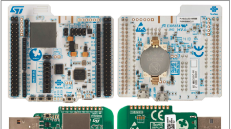
图6. Nucleo-68和USB dongle板外形图(左:正面;右:背面)
图7. Nucleo-68硬件框图

图. USB Dongle硬件框图
图 USB Dongle板外形图(正面)
图 USB Dongle板外形图(背面)
图. NUCLEO-WB55.Nucleo板电路图(1)
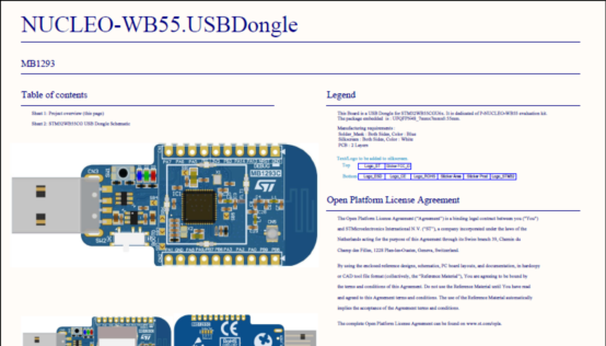
图.NUCLEO-WB55.USBDongle板电路图(1)
责任编辑:David
【免责声明】
1、本文内容、数据、图表等来源于网络引用或其他公开资料,版权归属原作者、原发表出处。若版权所有方对本文的引用持有异议,请联系拍明芯城(marketing@iczoom.com),本方将及时处理。
2、本文的引用仅供读者交流学习使用,不涉及商业目的。
3、本文内容仅代表作者观点,拍明芯城不对内容的准确性、可靠性或完整性提供明示或暗示的保证。读者阅读本文后做出的决定或行为,是基于自主意愿和独立判断做出的,请读者明确相关结果。
4、如需转载本方拥有版权的文章,请联系拍明芯城(marketing@iczoom.com)注明“转载原因”。未经允许私自转载拍明芯城将保留追究其法律责任的权利。
拍明芯城拥有对此声明的最终解释权。
相关资讯
:
基于MC33771主控芯片的新能源锂电池管理系统解决方案

AMIC110 32位Sitara ARM MCU开发方案

基于AMIC110多协议可编程工业通信处理器的32位Sitara ARM MCU开发方案

基于展讯SC9820超低成本LTE芯片平台的儿童智能手表解决方案

基于TI公司的AM437x双照相机参考设计

基于MTK6580芯片的W2智能手表解决方案


 2012- 2022 拍明芯城ICZOOM.com 版权所有 客服热线:400-693-8369 (9:00-18:00)


