


 产品分类
产品分类
TI OMAP-L138低功耗应用处理器开发方案
 95
95
 拍明
拍明
原标题:TI OMAP-L138低功耗应用处理器开发方案
OMAP-L138 Low-Power Applications Processor
The device is a Low-power applications processor based on an ARM926EJ-S™ and a C674x DSP core. It provides significantly lower power than other members of the TMS320C6000™ platform of DSPs.
The device enables OEMs and ODMs to quickly bring to market devices featuring robust operating systems support, rich user interfaces, and high processing performance life through the maximum flexibility of a fully integrated mixed processor solution.
The dual-core architecture of the device provides benefits of both DSP and Reduced Instruction Set Computer (RISC) technologies, incorporating a high-performance TMS320C674x DSP core and an ARM926EJ-S core.
The ARM926EJ-S is a 32-bit RISC processor core that performs 32-bit or 16-bit instructions and processes 32-bit, 16-bit, or 8-bit data. The core uses pipelining so that all parts of the processor and memory system can operate continuously.
The ARM core has a coprocessor 15 (CP15), protection module, and Data and program Memory Management Units (MMUs) with table look-aside buffers. It has separate 16K-byte instruction and 16K-byte data caches. Both are four-way associative with virtual index virtual tag (VIVT). The ARM core also has a 8KB RAM (Vector Table) and 64KB ROM.
The device DSP core uses a two-level cache-based architecture. The Level 1 program cache (L1P) is a 32KB direct mapped cache and the Level 1 data cache (L1D) is a 32KB 2-way set-associative cache. The Level 2 program cache (L2P) consists of a 256KB memory space that is shared between program and data space. L2 also has a 1024KB Boot ROM. L2 memory can be configured as mapped memory, cache, or combinations of the two. Although the DSP L2 is accessible by ARM and other hosts in the system, an additional 128KB RAM shared memory is available for use by other hosts without affecting DSP performance.
The peripheral set includes: a 10/100 Mb/s Ethernet MAC (EMAC) with a Management Data Input/Output (MDIO) module; one USB2.0 OTG interface; one USB1.1 OHCI interface; two inter-integrated circuit (I2C) Bus interfaces; one multichannel audio serial port (McASP) with 16 serializers and FIFO buffers; two multichannel buffered serial ports (McBSP) with FIFO buffers; two SPI interfaces with multiple chip selects; four 64-bit general-purpose timers each configurable (one configurable as watchdog); a configurable 16-bit host port interface (HPI) ; up to 9 banks of 16 pins of general-purpose input/output
(GPIO) with programmable interrupt/event generation modes, multiplexed with other peripherals; three UART interfaces (each with RTS and CTS); two enhanced high-resolution pulse width modulator (eHRPWM) peripherals; 3 32-bit enhanced capture (eCAP) module peripherals which can be configured as 3 capture inputs or 3 auxiliary pulse width modulator (APWM) outputs; and 2 external memory interfaces: an asynchronous and SDRAM external memory interface (EMIFA) for slower memories or peripherals, and a higher speed DDR2/Mobile DDR controller.
The Ethernet Media Access Controller (EMAC) provides an efficient interface between the device and a network. The EMAC supports both 10Base-T and 100Base-TX, or 10 Mbits/second (Mbps) and 100 Mbps in either half- or full-duplex mode. Additionally an Management Data Input/Output (MDIO) interface is available for PHY configuration. The EMAC supports both MII and RMII interfaces.
The SATA controller provides a high-speed interface to mass data storage devices. The SATA controller supports both SATA I (1.5 Gbps) and SATA II (3.0 Gbps).
The Universal Parallel Port (uPP) provides a high-speed interface to many types of data converters, FPGAs or other parallel devices. The UPP supports programmable data widths between 8- to 16-bits on each of two channels. Single-date rate and double-data rate transfers are supported as well as START, ENABLE and WAIT signals to provide control for a variety of data converters.
A Video Port Interface (VPIF) is included providing a flexible video input/output port. The rich peripheral set provides the ability to control external peripheral devices and communicate with external processors. For details on each of the peripherals, see the related sections later in this document and the associated peripheral reference guides.
The device has a complete set of development tools for the ARM and DSP. These include C compilers, a DSP assembly optimizer to simplify programming and scheduling, and a Windows™ debugger interface for visibility into source code execution.
OMAP-L138主要特性:
Dual Core SoC
300-MHz ARM926EJ-S™ RISC MPU
300-MHz C674x VLIW DSP
ARM926EJ-S Core
32-Bit and 16-Bit (Thumb®) Instructions
DSP Instruction Extensions
Single Cycle MAC
ARM® Jazelle® Technology
EmbeddedICE-RT™ for Real-Time Debug
ARM9 Memory Architecture
C674x Instruction Set Features
Superset of the C67x+™ and C64x+™ ISAs
2400/1800 C674x MIPS/MFLOPS
Byte-Addressable (8-/16-/32-/64-Bit Data)
8-Bit Overflow Protection
Bit-Field Extract, Set, Clear
Normalization, Saturation, Bit-Counting
Compact 16-Bit Instructions
C674x Two Level Cache Memory Architecture
32K-Byte L1P Program RAM/Cache
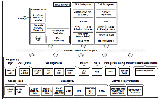
图1。OMAP-L138功能方框图
The DSP Subsystem includes the following features:
·C674x DSP CPU
·32KB L1 Program (L1P)/Cache (up to 32KB)
·32KB L1 Data (L1D)/Cache (up to 32KB)
·256KB Unified Mapped RAM/Cache (L2)
·1MB Mask-programmable ROM
·Little endian
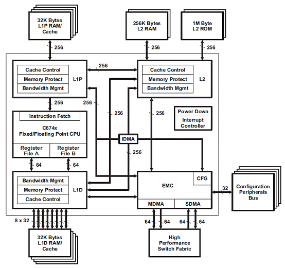
图2。C674x CPU方框图
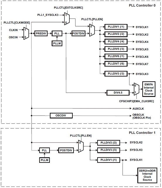
图3。OMAP-L138 PLL拓扑图

图4。OMAP-L138 I2C模块方框图
Hawkboard is an open community board mainly designed to provide to the community a feature rich & economical solution based on Ti s OMAP L138 processor. With a wide range of peripheral support, this board is an ultimate tool for digital media & storage applications。
The OMAP L138 offers an integrated ARM9 and a Ti DSP. Its low power consumption level opens this system to a large range of Embedded & industrial applications.
Internal Memory controller offers support for wide range of memories including DDR2/MDDR/SDRAM/NOR & NAND FLASH.
Inbuilt SATA controller supporting SATA I & SATA II interfaces are available for extending the storage capacity of this platform. Inbuilt MMC/SD controller provides an instant add on storage for personal collections.
UPP provides a high speed parallel interface to FPGAs & other data converters.
Two USB ports provide wide variety of peripheral connectivity. The USB OTG port also provides an option to power the Hawkboard when connected to a PC/LAPTOP.
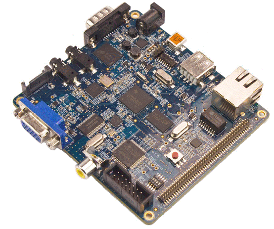
图5。Hawkboard开发板外形图
Hawkboard开发板主要特性:
Processor
·Ti OMAP-L138 Low Power Application Processor
·300-MHz ARM926EJ-STM RISC CPU
·300-MHz C674x VLIW DSP
·On-Chip RTC
Memory
·128 MByte DDR2 SDRAM running at 150MHz
·128 MByte NAND FLASH
·1 SD/MMC Slot
Interfaces
·One RS232 Serial Port
·One Fast Ethernet Port (10/100 Mbps)
·One USB Host port (USB 1.1)
·One USB OTG port (USB 2.0)
·One SATA Port (3Gbps)
·One VGA Port (15 pin D-SUB)
·Two AUDIO Ports (1 LINE IN & 1 LINE OUT)
·One Composite IN (RCA Jack)
Expansion Interface
·VPIF
·UPP
·PRU
·LCDC
·UART(x2)
·SPI (x2)
·I2C (x1)
·eCAP
·eHRPWM
·GPIO
Software Support
·U-Boot
·Linux BSP
Hawkboard开发板主要特性和优势:
Features(特性)Benefits(优势)
OMAP-L138 processor integrates an ARM 926 applications processor and C674x floating-point digital signal processor, delivering up to 450 MHz performanceTwo processors in a single package increase board space savings and offer developers processing efficiency by allowing the ARM to support complex operating systems and the DSP to handle high-precision data processing
128 MB of DDR2 RAM and 128 MB of NAND flashLarge on-board memory allows developers to run multiple applications on an open platform
Built-in SATA controller supports SATA I and II interfaces as well as built-in MMC/SDAllows developers to connect a high capacity storage drive or other memory interfaces
JTAG interfaceProvides low-level debugging and reads/writes software and data into system memories
Two integrated USB ports, including USB on-the-go (OTG)Power can be driven by PC or laptop, and developers can easily plug and play other USB-enabled devices
Stereo audio in/out and video (VGA) in/out interfacesFacilitates a seamless audio and video experience
Contains serial interfaces and additional expansion ports (SPI, UPP, PRU, VPIF, GPIO, UART, I2C, LCDC, eCAP and eHRPWM)Allows communication with numerous devices and customization for proprietary interface
责任编辑:David
【免责声明】
1、本文内容、数据、图表等来源于网络引用或其他公开资料,版权归属原作者、原发表出处。若版权所有方对本文的引用持有异议,请联系拍明芯城(marketing@iczoom.com),本方将及时处理。
2、本文的引用仅供读者交流学习使用,不涉及商业目的。
3、本文内容仅代表作者观点,拍明芯城不对内容的准确性、可靠性或完整性提供明示或暗示的保证。读者阅读本文后做出的决定或行为,是基于自主意愿和独立判断做出的,请读者明确相关结果。
4、如需转载本方拥有版权的文章,请联系拍明芯城(marketing@iczoom.com)注明“转载原因”。未经允许私自转载拍明芯城将保留追究其法律责任的权利。
拍明芯城拥有对此声明的最终解释权。
相关资讯
:
基于MC33771主控芯片的新能源锂电池管理系统解决方案

AMIC110 32位Sitara ARM MCU开发方案

基于AMIC110多协议可编程工业通信处理器的32位Sitara ARM MCU开发方案

基于展讯SC9820超低成本LTE芯片平台的儿童智能手表解决方案

基于TI公司的AM437x双照相机参考设计

基于MTK6580芯片的W2智能手表解决方案


 2012- 2022 拍明芯城ICZOOM.com 版权所有 客服热线:400-693-8369 (9:00-18:00)


