


 产品分类
产品分类
Renesas RE01 Group系列32位ARM MCU开发方案
 170
170
 拍明
拍明
原标题:Renesas RE01 Group系列32位ARM MCU开发方案
Renesas公司的RE01 Group系列是采用创新的SOTB™工艺,具有超低的工作电流和超低的待机电流,低压1.2V时具有高工作频率,最大64MHz.器件集成了32位Arm® Cortex®-M0+ mcu,1.5MB闪存,256KB SRAM,能量收获控制电路,MIP LCD控制器,2D图像引擎,14位超低功耗ADC,基准电压发生电路,RTC,次时钟修正电路,安全功能(可选),USB 2.0全速模块,SPI和quad SP.主要用在可穿戴设备,家用电器,建筑物自动化,工业传感器设备,智能锁,资产跟踪器和其它应用.本文介绍了RE01 Group主要特性,Cortex-M0+ CPU 框图,RE01 Group框图以及评估板RE01 1500KB主要特性和指标与MIP-LCD扩展板指标,主板布局图和MIP-LCD扩展板布局图,以及主板电路图和MIP-LCD扩展板电路图.
The RE01 Group uses Renesas’ innovative SOTB™ process technology and realizes both ultra-low active current and ultra-low standby current, and high-speed operation (maximum 64MHz) at low voltage (1.62V), which is impossible with a conventional bulk transistor, and is an embedded controller that can operate by energy harvesting. It is equipped with an energy harvesting control circuit, ultra-low power consumption 14-bit ADC (approx. 4uA), flash (rewrite at less than 1mA), parallel MIP-LCD interface, 2D graphics, UI for clock movement, and security functions such as a trusted secure IP. It also has large-capacity 1.5MB flash and 256KB SRAM that can handle data logging and firmware updates. Therefore, the RE01 Group is suitable for wearable devices, home appliances, building automation, industrial sensor devices, smart locks, asset trackers, and other applications.
RE01 GroupCPU
Arm® Cortex-M0+
- Revision: r0p1-00rel0
- Arm®v6-M architecture profile
- Single-cycle integer multiplier
Memory Protection Units (MPU)
- Arm®v6 Protected Memory System Architecture
- Eight protected regions
SysTick timer
- Driven by LOCO clock (32.768 kHz ± 30%)
Debug
Arm® CoreSight™ MTB-M0+
- Revision: r0p1-00rel0
- Buffer size: 32-Kbyte MTB RAM
Data Watchpoint Unit (DWT)
- Two comparators for watchpoints
Breakpoint Unit (BPU)
- Four instruction comparators
CoreSight Debug Access Port (DAP)
- Serial Wire Debug Port (SW-DP)
Debug Register Module (DBGREG)
- Reset control
- Stop control
Operating frequency
CPU core: maximum 64 MHz
Serial Wire Data (SWD) interface: maximum 12.5 MHz
RE01 Group主要特性:
■ Arm® Cortex®-M0+ core incorporated
Maximum operating frequency: 64 MHz (boost mode)
ARM® Memory Protection Unit (MPU)
CoreSight™ debug port: SW-DP
■ Power-saving functions
Back-bias control function based on silicon-on-thin-buried-oxide(SOTB™) process technology
Operation at ultra-low power-supply voltages (from 1.62 V to 3.6 V)
Four power control modes based on the operating frequency
Four low power consumption modes
Three power supply modes
■ On-chip code flash memory
1.5-Mbyte code flash memory
Background programming/erasing
No cycles of waiting for access in operation at or below 32 MHz;one cycle of waiting at frequencies above 32 MHz
Function for area protection prevents erroneous overwriting ortampering
■ On-chip SRAM
256-Kbyte SRAM with no access wait cycles
■ Data transfer
Four DMA controllers
Single data transfer controller (DTC)
■ Reset and supply management
Power-on reset circuit (POR)
Low voltage detection (LVD) can be set.
■ Multiple clock sources
External crystal oscillator (main clock): 8 to 32 MHz
External crystal oscillator (sub-clock): 32.768 kHz
High-speed on-chip oscillator (HOCO): 24, 32, 48, or 64 MHz
Middle-speed on-chip oscillator (MOCO): 2 MHz
Low-speed on-chip oscillator (LOCO): 32 kHz
Independent watchdog timer on-chip oscillator: 16 kHz
PLL frequency synthesizer
■ Energy harvesting control
A power generation element is directly connectable.
High-speed startup is possible without having to wait for the chargingof a secondary battery.
Function to prevent a secondary battery from overcharging
■ Independent watchdog timer
14-bit counter, 16-kHz (1/2 LOCO clock frequency) operation
■ Sub-clock correction circuit (CCC)
The CCC corrects the accuracy of oscillation every 16 seconds(theoretical regulation).
Events can be generated per second in deep software standby mode.
■ Communication functions
Single USB 2.0 full-speed host/function module with PHY layer
Two serial peripheral interfaces
Single 128-bit buffer for which up to eight commands can be specified
Single 32-bit buffer for which one command can be specified
Single quad serial peripheral interface connectable to an external flashmemory
Two I2C bus interfaces
Five serial communications interfaces (SCIg)
Asynchronous, clock-synchronous, simple I2C, simple SPI, and smart
card interfaces, and IrDA interface version 1.0 (the latter is onlyapplicable to SCI0)
Two serial communication interfaces (SCIi) each having a 16-byteFIFO
■ Various analog circuits
Single 14-bit successive approximation A/D converterHigh precision: 7 channels, standard precision: 11 channels
Single 12-bit D/A converter with a buffer amplifier
Single analog comparator (ACMP)
Single temperature sensor for measuring the internal temperature of thechip
Reference voltage generation circuit for the 14-bit A/D converter
Single motor driver control circuit (MTDV)
The MTDV can drive up to three motors.
Single constant current (1 mA or 0.5 mA) source circuit with threechannels that can drive three external LEDs
■ Various timer circuits
Six general PWM timers (GPT)
Two 32-bit counters
Four 16-bit counters
Two asynchronous general-purpose timers (AGT) that can be used instandby mode
Two 8-bit timers (TMR)
Single realtime clock (RTC)
Single watchdog timer (WDT)
Single low-speed timer (LST) that operates at 1 kHz
A circuit for converting hexadecimal numbers to decimal numbers foruse as a stopwatch
Single low-speed pulse generator (LPG)
Pulse output at two frequencies (2.048 or 4.096 kHz) is possible.
■ Human machine interfaces
Single memory-in-pixel (MIP) LCD controller (MLCD)Parallel interface is supported.
Single 2D graphics data conversion circuit (GDT)
■ Security functions (optional)
Single Trusted Secure IP Lite (TSIP)
· AES (128- or 256-bit key length, supporting ECB, CBC, CMAC,GCM, and others)
· Key wrapping protects against the leakage of the encryption keysof users.
· An access management circuit disables illicit access to theencryption engine.
· Using the other security functions together with area protectionenables secure booting and secure over-the-air (OTA) softwareupdates.
■ Operating voltage and temperature range
VCC = IOVCC = 1.62 V to 3.6 V
IOVCCn and AVCCn can each be independently set to a voltagewithin the range between 1.62 V and 3.6 V.
Ta: –40 to +85 ℃
RE01 Group主要应用:
The RE01 group enables energy harvesting for any IoT device, eliminating the need for battery replacement / maintenance. SOTB-powered ultra-low power 32-bit CPU realizes smart IoT devices powered by an even tiny ambient power source.
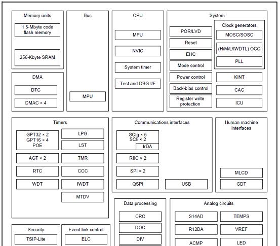
图.RE01 Group框图
评估板RE01 1500KB
Evaluation Kit RE01 1500KB allows for evaluation and development by combining energy harvesting with the user’s hardware system, which makes semi-permanent battery maintenance for the RE01 1500KB unnecessary.
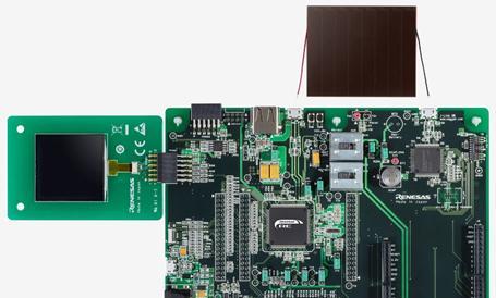
图.评估板RE01 1500KB外形图
评估板RE01 1500KB主要特性:
Energy harvesting system: can be evaluated with the power generation elements, the secondary battery connection interface, and the sample code provided by Renesas.*1
Arduino Uno Header and PMOD interface supported: enable evaluation of energy harvesting system combined with the user’s hardware system.
On-board debug function supported: enable program debugging by simply connecting the included USB cable to a host PC.
评估板RE01 1500KB包括:
Evaluation Board RE01 1500KB
PMOD-compatible low-power LCD (Memory-In-Pixel LCD) expansion board
Solar panel
USB cable (Micro-B)
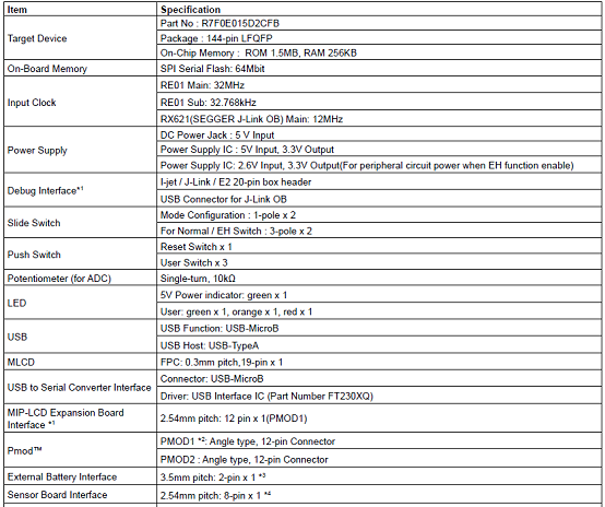
评估板RE01 1500KB主要指标:
责任编辑:David
【免责声明】
1、本文内容、数据、图表等来源于网络引用或其他公开资料,版权归属原作者、原发表出处。若版权所有方对本文的引用持有异议,请联系拍明芯城(marketing@iczoom.com),本方将及时处理。
2、本文的引用仅供读者交流学习使用,不涉及商业目的。
3、本文内容仅代表作者观点,拍明芯城不对内容的准确性、可靠性或完整性提供明示或暗示的保证。读者阅读本文后做出的决定或行为,是基于自主意愿和独立判断做出的,请读者明确相关结果。
4、如需转载本方拥有版权的文章,请联系拍明芯城(marketing@iczoom.com)注明“转载原因”。未经允许私自转载拍明芯城将保留追究其法律责任的权利。
拍明芯城拥有对此声明的最终解释权。
相关资讯
:
基于MC33771主控芯片的新能源锂电池管理系统解决方案

AMIC110 32位Sitara ARM MCU开发方案

基于AMIC110多协议可编程工业通信处理器的32位Sitara ARM MCU开发方案

基于展讯SC9820超低成本LTE芯片平台的儿童智能手表解决方案

基于TI公司的AM437x双照相机参考设计

基于MTK6580芯片的W2智能手表解决方案


 2012- 2022 拍明芯城ICZOOM.com 版权所有 客服热线:400-693-8369 (9:00-18:00)


