


 产品分类
产品分类
Silabs Si5391宽带PLL和高性能时钟发生器解决方案
 315
315
 拍明
拍明
原标题:Silabs Si5391宽带PLL和高性能时钟发生器解决方案
Silabs公司的Si5391是采用新一代MultiSynth技术的宽带PLL,能提供业界最多种类和高性能的时钟发生器.PLL锁住XA/XB间的外接晶振或连接到XA/XB或IN0,1,2的外接时钟.分数或整数的倍频器选择输入时钟或晶振频率高达很高的频率,由MultiSynth输出级进行分频到输出端100 Hz 到1 GHz间的任一频率.MultiSynth级能由分数或整数值进行分频,高分辨率MultiSynth分频器能使真正的任一输入频率到输出端的任一频率.输出分频器提供灵活的输出格式,可以在每个输出端进行独立配置.该时钟发生器完全通过串行接口(I2C/SPI)和电路中可编程非易失存储器进行配置.Si5391具有超低抖动性能,精密校准是为69fs RMS,整数模式为75fs RMS,分数模式为115fs RMS,输入频率为外接晶振(25MHz-54MHz),差分时钟为10 - 750 MHz, LVCMOS时钟为10 到 250 MHz;输出频率范围,差分为100 Hz - 1028 MHz, LVCMOS为100 Hz - 250 MHz,高度可配置输出和LVDS, LVPECL, LVCMOS, CML以及HCSL兼容,并可编程信号幅度.主要用在100G/200G/400G应用上.本文介绍了Si5391主要特性和详细特性,功能框图,SerDes应用框图以及评估板Si5391A-A-EVB主要特性,框图和连接图,电路图,材料清单和PCB设计图.
The Si5391 combines a wide band PLL with next generation MultiSynth technology to offer the industry’s most versatile and high performanceclock generator. The PLL locks to either an external crystal between XA/XB or to an external clock connected to XA/XB or IN0, 1, 2. A fractional or integer multiplier takes the selected input clock or cystal frequency up to a very high frequency that is thendivided by the MultiSynth output stage to any frequency in the range of 100 Hz to 1 GHz on each output. The MultiSynth stage candivide by both integer and fractional values. The high-resolution fractional MultiSynth dividers enable true any-frequency input to anyfrequencyon any of the outputs. The output drivers offer flexible output formats which are independently configurable on each of theoutputs. This clock generator is fully configurable via its serial interface (I2C/SPI) and includes in-circuit programmable non-volatilememory.
The any-frequency, any-output Si5391 clock generators combine a wide-band PLL with proprietaryMultiSynth™ fractional synthesizer technology to offer a versatile and high performance clock generator platform. This highly flexible architecture is capable of synthesizing a wide range of integer and non-integer related frequencies up to 1 GHz on 12 differential clock outputs while delivering sub-100 fs rms phase jitter performance optimized for 100G/200G/400G applications. Each of the clock outputs can be assigned its own format and output voltage enabling the Si5391 to replace multiple clockICs and oscillators with a single device making it a true "clock tree on a chip."
The Si5391 can be quickly and easily configured using ClockBuilderPro software. Custom part numbers are automatically assigned using ClockBuilder Pro™ for fast, free,and easy factory pre-programming or the Si5391 can be programmed via I2C and SPIserial interfaces.
Si5391主要特性:
• Generates any combination of outputfrequencies from any input frequency
• Ultra-low jitter performance
• 69fs RMS (Precision Calibration)
• 75fs RMS (integer mode)
• 115fs RMS (fractional mode)
• Input frequency range:
• External crystal: 25 to 54 MHz
• Differential clock: 10 to 750 MHz
• LVCMOS clock: 10 to 250 MHz
• Output frequency range:
• Differential: 100 Hz to 1028 MHz
• LVCMOS: 100 Hz to 250 MHz
• Highly configurable outputs compatible withLVDS, LVPECL, LVCMOS, CML, and HCSL with programmable signal amplitude
• Si5391: 4 input, 12 output, 64-QFN 9x9mm
Si5391应用:
• 100/200/400G switches
• 56G/112G PAM4 SerDes reference clocks
• Clock tree generation replacing XOs, buffers, signal format translators
• Clocking for FPGAs, processors, memory
• Ethernet switches/routers
• OTN framers/mappers/processors
Si5391详细特性如下:
• Generates any combination of output frequencies from any inputfrequency
• Ultra-low phase jitter performance
• 69fs RMS (Precision Calibration)
• 75fs RMS (integer mode)
• 115fs RMS (fractional mode)
• Input frequency range:
• External crystal: 25 to 54 MHz
• Differential clock: 10 to 750 MHz
• LVCMOS clock: 10 to 250 MHz
• Output frequency range:
• Differential: 100 Hz to 1028 MHz
• LVCMOS: 100 Hz to 250 MHz
• Highly configurable outputs compatible with LVDS, LVPECL,LVCMOS, CML, and HCSL with programmable signal amplitude
• Optional zero delay mode
• Glitchless on the fly output frequency changes
• DCO mode: as low as 0.001 ppb steps
• Core voltage
• VDD: 1.8 V ±5%
• VDDA: 3.3 V ±5%
• Independent output clock supply pins
• 3.3 V, 2.5 V, or 1.8 V
• Serial interface: I2C or SPI
• In-circuit programmable with non-volatile OTP memory
• ClockBuilder Pro software simplifies device configuration
• 64-QFN 9x9mm
• Temperature range: –40 to +85 ℃
• Pb-free, RoHS-6 compliant
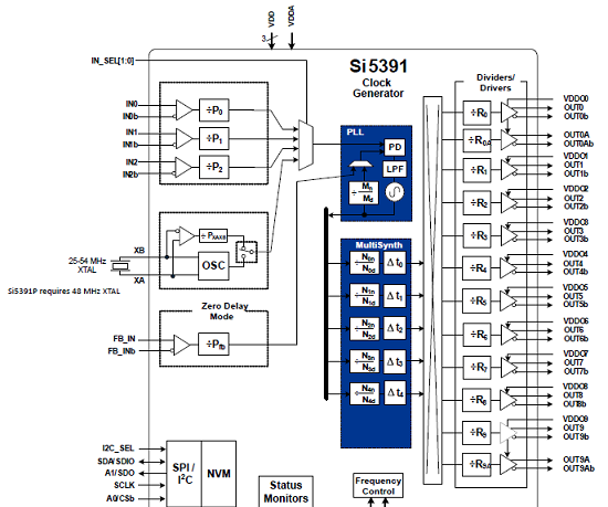
图1.Si5391框图
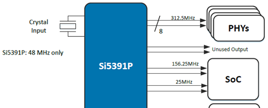
图2.Si5391P 56G SerDes应用框图
评估板Si5391A-A-EVB
The Si5391A-A-EVB is used for evaluating the Si5391A Any-Frequency, Any-Output, Jitter-Attenuating Clock Multiplier revision D. The device revision is distinguished by a white 1 inch x 0.187 inch label with the text “SI5391-A-EB” installed in the lower left hand corner of the board. (For ordering purposes only, the terms “EB” and “EVB” refer to the board and the kit respectively.
评估板Si5391A-A-EVB主要特性:
• Powered from USB port or external powersupply.
• Onboard 48 MHz XTAL allows free-runmode of operation on the Si5391A or up to3 input clocks for synchronous clocking.
• Feedback clock input for optional zerodelay mode.
• ClockBuilder® (CBPro) GUI programmableVDD supply allows device to operate from 3.3, 2.5, or 1.8 V.
• CBPro GUI programmable VDDO suppliesallow each of the 10 outputs to have its own power supply voltage selectable from3.3, 2.5, or 1.8 V.
• CBPro GUI-controlled voltage, current, andpower measurements of VDD and all
VDDO supplies.
• Status LEDs for power supplies andcontrol/status signals of Si5391A.
• SMA connectors for input and outputclocks.
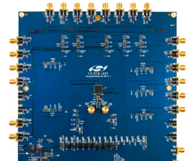
图3.评估板Si5391A-A-EVB外形图
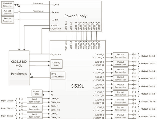
图4.评估板Si5391A-A-EVB功能框图
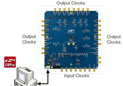
图5.评估板Si5391A-A-EVB连接图
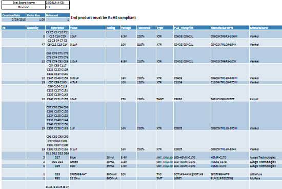
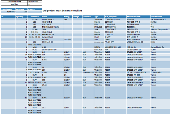
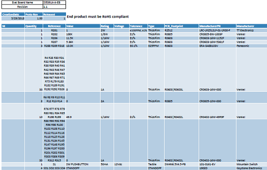
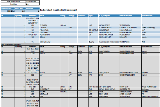
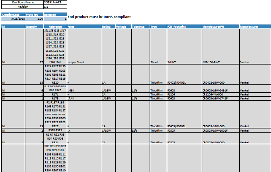
评估板Si5391A-A-EVB材料清单:
责任编辑:David
【免责声明】
1、本文内容、数据、图表等来源于网络引用或其他公开资料,版权归属原作者、原发表出处。若版权所有方对本文的引用持有异议,请联系拍明芯城(marketing@iczoom.com),本方将及时处理。
2、本文的引用仅供读者交流学习使用,不涉及商业目的。
3、本文内容仅代表作者观点,拍明芯城不对内容的准确性、可靠性或完整性提供明示或暗示的保证。读者阅读本文后做出的决定或行为,是基于自主意愿和独立判断做出的,请读者明确相关结果。
4、如需转载本方拥有版权的文章,请联系拍明芯城(marketing@iczoom.com)注明“转载原因”。未经允许私自转载拍明芯城将保留追究其法律责任的权利。
拍明芯城拥有对此声明的最终解释权。
相关资讯
:
基于MC33771主控芯片的新能源锂电池管理系统解决方案

AMIC110 32位Sitara ARM MCU开发方案

基于AMIC110多协议可编程工业通信处理器的32位Sitara ARM MCU开发方案

基于展讯SC9820超低成本LTE芯片平台的儿童智能手表解决方案

基于TI公司的AM437x双照相机参考设计

基于MTK6580芯片的W2智能手表解决方案


 2012- 2022 拍明芯城ICZOOM.com 版权所有 客服热线:400-693-8369 (9:00-18:00)


