Power Integrations InnoSwitch3-MX 45W多输出电源参考设计DER-635
 236
236
 拍明
拍明
原标题:Power IntegrationsInnoSwitch3-MX 45W多输出电源参考设计DER-635
Power Integrations公司的InnoSwitch3-MX是最新的反激隔离开关系列,组合了初级FET,初级控制器,用于同步整流的次级控制器,以及高速通信技术,不需要光耦合器;而InnoSwitch3-MX接收来自InnoMux集成电路的控制信息,能单独测量每个输出的负荷要求,指导InnoSwitch3-MX开关为每个输出提供正确的输出量,以维持电流或电压的精确管理,这就消除了以前常见的负载和交叉调节.因此,InnoSwitch3-MX的架构集成了初级和次级控制器,大大地简化多个输出电源开发和制造,特别是那些紧凑外壳和高效率要求的多输出电源.主要用在满足能量之星8和CEC的监视器和LED电视机(TV).本文介绍了InnoSwitch3-MX产品亮点,初级控制器框图和次级控制器框图,以及采用InnoMUXTMIMX111U和InnoSwitchTM3-MX INN3468C的有两个 CV和一个CC的45W多输出反激转换器的参考设计DER-635主要指标,高等级电路图,以及参考设计DER-635电路图,材料清单和变压器电路图,建造图,连接框图和PCB设计图.
The InnoSwitch3-MX dramatically simplifies the development andmanufacturing of multiple output power supplies, particularly those incompact enclosures or with high efficiency requirements. TheInnoSwitch3-MX architecture is revolutionary in that the devicesincorporate both prIMAry and secondary controllers, with senseelements and a safety-rated feedback mechanism into a single IC.
Close component proximity and innovative use of the integratedcommunication link, FluxLink, permit accurate control of a secondarysidesynchronous rectification MOSFET with Quasi-Resonant switchingof primary integrated high-voltage switch to maintain high efficiencyacross the entire load range.
This version of InnoSwitch3 is intended to be used with InnoMux formultiple output, single-stage power supplies for monitors and TVs.This enables very high system efficiency on a small PCB foot print.
The InnoSwitch3-MX combines a high-voltage power switch, alongwith both primary-side and secondary-side controllers in one device.
The InnoSwitch3-MX is intended to be paired with an InnoMuxcontroller.The InnoSwitch3-MX architecture incorporates a novel inductivecoupling feedback scheme using the package leadframe and bondwires to provide a safe, reliable, and low-cost means to accuratelycommunicate power requests from the InnoMux controller to theprimary controller.
The primary controller on InnoSwitch3-MX is a quasi-resonant (QR)flyback controller that has the ability to operate in continuousconduction mode (CCM). The controller uses a variable currentcontrol scheme. The primary consists of a jitter oscillator; a receivercircuit magnetically coupled to the secondary controller, a currentlimit controller, 5 V regulator on the PRIMARY BYPASS pin, audiblenoise reduction engine, bypass overvoltage detection circuit, alossless input line sensing circuit, current limit selection circuitry,overvoltage protection, leading edge blanking, secondary outputdiode / SR MOSFET short protection circuit and a 650 V / 725 V /750 V power switch.
The secondary controller consists of a transmitter circuit that is magnetically coupled to the primary receiver, synchronous rectifier (SR) MOSFET driver, timing functions and a host of integrated protection features.
InnoSwitch3-MX产品亮点:
Based on InnoSwitch3
• Partner IC to InnoMux
• High efficiency across full load range
• Incorporates a multi-mode Quasi-Resonant (QR) / CCM flybackcontroller, 650 V or 725 V switch, secondary-side sensing andsynchronous rectification driver
• Integrated FluxLink™, HIPOT-isolated, feedback link
• Instantaneous transient response ±5% CV with 0%-100%-0%load step
EcoSmart™ – Energy Efficient
• Easily meets all global energy efficiency regulations
• Low heat dissipation
Advanced Protection / Safety Features
• Primary sensed output OVP
• Open SR FET gate detection
• Hysteretic thermal shutdown
• Input voltage monitor with accurate brown-in/brown-out andovervoltage protection
Full Safety and Regulatory Compliance
• Reinforced insulation
• Isolation voltage >4000 VAC
• 100% production HIPOT compliance testing
• UL1577 and TUV (EN60950) safety approved
• Enables designs that have “A” performance criteria for EN61000-4suite of test standards, including EN61000-4-2, 4-3 (30 V/m), 4-4,4-5, 4-6, 4-8 (100 A/m) and 4-9 (1000 A/m)
Green Package
• Halogen free and RoHS compliant
InnoSwitch3-MX应用:
• Use with InnoMux for Energy Star 8 and CEC for monitors and TVs
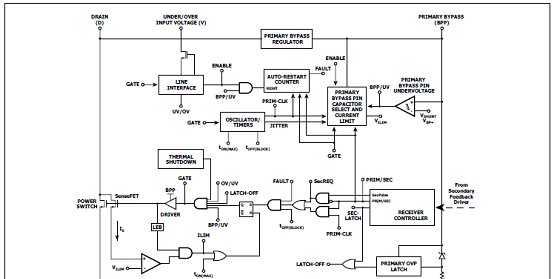
图1.InnoSwitch3-MX初级框图
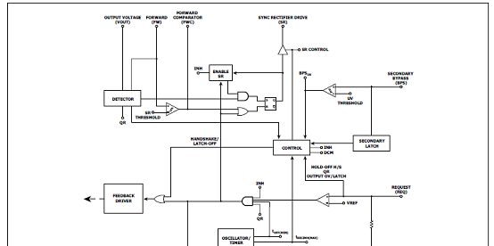
图2.InnoSwitch3-MX次级框图
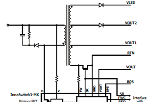
图3. InnoSwitch3-MX典型应用/性能框图
采用InnoMUXTMIMX111U和InnoSwitchTM3-MX INN3468C的有两个CV和一个CC的45W多输出反激转换器参考设计DER-635
This engineering report describes a PSU for a LED TV. This Switch Mode Power Supply (SMSP), utilizes InnoSwitch3-MX and InnoMUX from the InnoSwitch family. It has a 5 V / 1 A and 12 V / 1.25 A outputs and 25 W output providing power to one CC driver intended for LED back-light in the TV panel. The total current hrough the LED strings is controlled from 0mA to 650mA by an analogue signal (ADIM) with a full scale of 1.5 V. The total maximum power output is 45W and the input voltage range is 90 VAC to 265 VAC.
The new architecture uses a multiplexed system where only one transformer as shown in Figureure4. For each switching cycle, the energy stored in the transformer during the primary conduction interval is delivered to only one of the converter ’s main outputs (CV1, CV2 or LED). Leveraging only a single magnetic component, the controller directs the energy flow as needed to all outputs based on respective loading requirements, thus keeping each output accurately controlled. This multiplexing is achieved by gating the steering FET Q2 or Q4 appropriately. If energy pulse needs to be delivered to the CV1 output, Q2 it turned ON prior to the end of the primary conduction interval. Same process for CV2 with Q4 steering FET, otherwise If Q1 and Q4 are held OFF the energy will be delivered to the LED output via the rectification diode D3.
InnoSwitch3-MX and InnoMUX are industry first AC/DC ICs chipset with isolated, safety rated integrated feedback. In addition there are a built in synchronous rectification for >90% efficiency at nominal AC input.
The control chipset incorporates isolated feedback and communication channels while implementing All the benefits of secondary-side control with the simplicity of primary-side regulation.
There are a few important safety feature, such as
• Output overvoltage protection (OVP), which eliminates the need for fault protection optocoupler.
• Accurate thermal protection with hysteretic shutdown.
• Input voltage monitor with accurate brown-in/brown-out and overvoltage protection.
The new architecture goals are to achieve tight cross regulation across multiple outputs and high overall efficiency while simplifying the overall system by removing conventional DC-DC converter post-regulation stages. This one level converter enable to reduce board size significantly and part count shrinking in about 50% compare to conventional converter that require more than one extra converter level. In addition with this high level of integration we gain all the benefits of InnoSwitch protections from shorts to OVUV in the input or in the outputs terminals.
参考设计DER-635主要特性:
•Unique single stage conversion; multiple output; Flyback architecture enabling:
• High Efficiency across the universal line range
• Energy Star 8.0 efficiency compliance
• High accuracy independently regulated 5V/1A and 12V/1.25A CV outputs with extremely fast load transient response of 150μsec and 250μsec respectively.
• One CC LED output with wide string voltage range of 30-50V makes it suitable for wide range of Televisions applications.
• Configurable for
oanalogue dimming mode
oStraight PWM dimming mode
oFiltered PWM dimming mode and
oHybrid dimming mode.

图4.参考设计DER-635高等级电路图
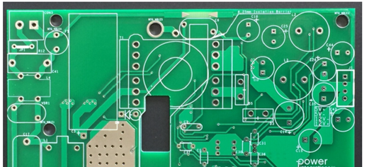
图5.参考设计DER-635 PCB正面视图
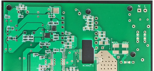
图6.参考设计DER-635 PCB背面视图
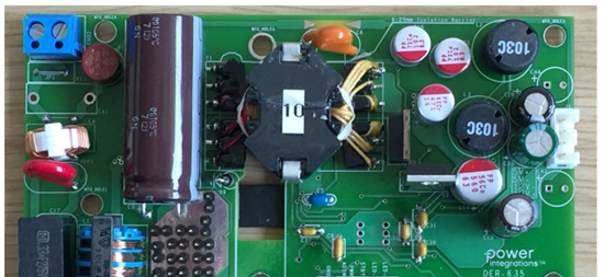
图7.参考设计DER-635 PCB装图:正面
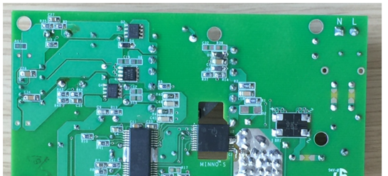
图8.参考设计DER-635 PCB装配图:背面
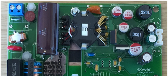
图9.参考设计DER-635 冷却装配图:正面
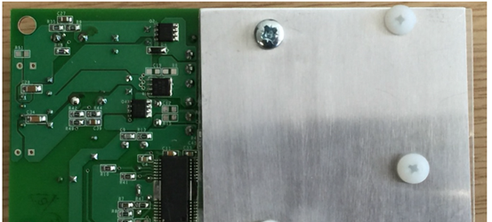
图10.参考设计DER-635 冷却装配图:背面
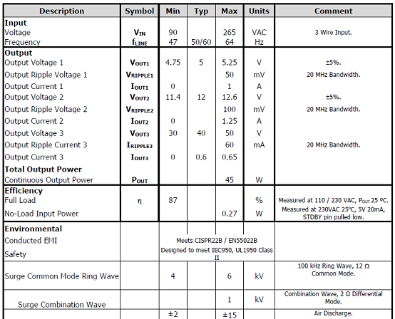
参考设计DER-635主要指标:
参考设计DER-635材料清单:
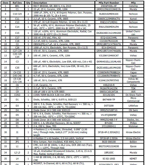
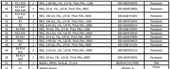
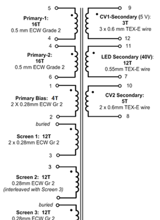
图12.参考设计DER-635变压器电路图
责任编辑:David
【免责声明】
1、本文内容、数据、图表等来源于网络引用或其他公开资料,版权归属原作者、原发表出处。若版权所有方对本文的引用持有异议,请联系拍明芯城(marketing@iczoom.com),本方将及时处理。
2、本文的引用仅供读者交流学习使用,不涉及商业目的。
3、本文内容仅代表作者观点,拍明芯城不对内容的准确性、可靠性或完整性提供明示或暗示的保证。读者阅读本文后做出的决定或行为,是基于自主意愿和独立判断做出的,请读者明确相关结果。
4、如需转载本方拥有版权的文章,请联系拍明芯城(marketing@iczoom.com)注明“转载原因”。未经允许私自转载拍明芯城将保留追究其法律责任的权利。
拍明芯城拥有对此声明的最终解释权。


 产品分类
产品分类




 2012- 2022 拍明芯城ICZOOM.com 版权所有 客服热线:400-693-8369 (9:00-18:00)


