Power Integrations InnoSwitch340W多输出反激转换器解决方案
 117
117
 拍明
拍明
原标题:Power Integrations InnoSwitch3 40W多输出反激转换器解决方案
Power Integrations公司的InnoSwitch3是基于氮化镓的AC/DC转换器集成电路,和InnoSwitch3-MX配对,InnoMux控制器由于用单级反激拓扑替代AC/DC和DC/DC转换器而大大简化了监视器和TV电源设计,使得电源系统在小的PCB占位面积得到非常高的效率,高达91%.LED背景光控制提供极好最小阈值调整,可选择模拟和几个PWM调光.而PWM调光则进一步提高了视觉功能,稳定了功率需求,并提供了扩展的保护特性.InnoMux控制器包括用于单独调整三个输出的多输出控制器,用来给InnoMux和一对InnoSwitch3-MX次级控制器供电的BP稳压器,用来直接把能量从变压器提供到合适输出的高边MOSFET驱动器, 防止不正常负载条件所引起的单独输出的分流器,驱动多达4个LED背景光串的电流源以及确定应用配置电阻值的阅读器.典型输出电压,一个CV模式为5-18V,两个CV模式为5V和12-18V,1-4个串LED背景光,LED串的电流匹配度为3%,高达100V串电压和高达960mA总串电流,高达2:1 LED串电压范围.模拟,PWM, 顺序脉宽调制和滤波PWM工作,主要用在能量之星8和监视器于TV的CEC.本文介绍了InnoSwitch3产品亮点,典型应用电路和控制器功能框图以及采用InnoMuxTMIMX102U和nnoSwitchTM3-MX INN3468C的40W多输出反激转换器主要特性,电源指标,电路图,变压器电路图,材料清单和PCB设计图.
When paired with InnoSwitch3-MX, InnoMux dramatically simplifies thepower supply design for monitors and TVs by replacing the ACDC andDCDC converters with a single-stage flyback topology. This enablesvery high system efficiency up to 91%, on a small PCB footprint.
The LED backlight control offers excellent minimum threshold regulationas well as analog and several PWM dimming options. The sequencedPWM dimming option further improves visual performance and stabilizespower demand. Extensive protection features are provided.
The InnoMux controller consists of a multi-output controller forregulating the three outputs independently, a BP Regulator for supplyingboth the InnoMux as well as the paired InnoSwitch3-MX secondarycontroller, High-Side MOSFET Drivers for directing the energyfrom the transformer to the appropriate output, Shunts to preventindividual outputs from rising in abnormal loading conditions, CurrentSources to drive up to four LED backlight strings, and Readers todetermine the value of application configuration resistors.
InnoSwitch3产品亮点:
CV and 4-Channel LED Backlight Controller
• Eliminates buck and LED backlight boost converters
• One or two constant voltage outputs
• Independently regulated outputs with instantaneous transientresponse ±5% CV on 0%-100%-0% load step
• Typical output voltages
• One CV mode: 5 V to 18 V
• Two CV mode: 5 V and 12 V to 18 V
• 1-4 string LED backlight
• 3% matching accuracy for LED strings
• Analog, PWM, sequenced PWM and filtered PWM operation
• Up to 100 V string voltage / up to 960 mA total string current
• Up to 2:1 LED string voltage range
Advanced Protection / Safety Features
• Individual overload protection for all outputs
• String imbalanced / short / open protection
• Output overvoltage set for auto-restart
Convenient Packages
• 28-Lead HSOP for single-sided wave soldered PCBs or small 28-Lead
QFN (5x5 mm Body) for compact multilayer designs
InnoSwitch3应用:
• ENERGY STAR 8 and CEC for monitors and TVs

图1.InnoSwitch3典型应用电路

图2.InnoMux控制器功能框图
采用InnoMuxTMIMX102U和nnoSwitchTM3-MX INN3468C的40W多输出反激转换器
This engineering report describes a PSU for a LED computer monitor. The 40 W PSU has a 5 V/3 A CV output and a 25 W output providing power to four CC drivers intended for back-light LED strings in the LED monitor. The current through the individual LED strings is controlled from 0 mA to 156 mA by an analogue signal (ADIM) with a full scale of 1.5 V. The total maximum power output is 40 W and the input voltage range is 90 VAC to 265 VAC.
The PSU is based on a multiplexed, single-stage, multiple output topology shown in Figure 1. For each switching cycle, the energy stored in the transformer during the primary conduction interval is delivered to only one of the converter’s main outputs (CV or LED). The energy from the primary is appropriately distributed between the converter main outputs by a secondary referred master controller according to the loading conditions at the outputs. This multiplexing is achieved by gating the steering FET Q1 appropriately. If energy pulse needs to be delivered to the CV1 output Q1 is turned ON prior to the end of the primary conduction interval. If Q1 is held OFF the energy is delivered to the LED output via the rectification diode D3. The master controller requests switching cycles from the primary as often as it needs to maintain all outputs in regulation. For the described multiplexing algorithm to work correctly it is essential that the transformer turns ratios are chosen such that: the minimum LED output voltage reflected to the primary of the transformer is greater than the CV output voltage reflected to the transformer primary. This technique achieves cross regulation within a fraction of 1% while significantly improving system efficiency when compared to conventional post regulation architectures. The new architecture supports multiple outputs driving both constant current and constant voltage loads, enabling the design of a single switch-mode power conversion stage that powers logic circuitry, USB ports, audio channels, and LED strings simultaneously.
This novel architecture is implemented using two controller ICs, the InnoSwitch3-MX IC for primary switching plus SR FET control, and InnoMux IC for output voltage and current control. Selection MOSFET Q1 and D3 are used to direct the energy packet to either the CV or LED output respectively.
40W多输出反激转换器主要特性:
Unique single stage conversion; multiple outputs; flyback architecture
• High full power efficiency across the universal line range
• Energy Star 8.0 efficiency compliance
• High accuracy independently regulated 5 V/3 A CV output with extremely fast load transient response.
• Four independent CC LED outputs matched to within <3.5% at full current.
• Wide LED string voltage range: 30 V to 50 V makes it suitable for wide range of computer monitor applications.
• Configurable for o Analog dimming mode
o Straight PWM dimming mode
o Filtered PWM dimming mode
o Hybrid dimming mode
• Control chipset incorporating isolated feedback and communication channels
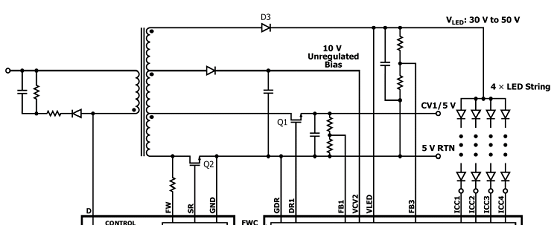
图3.复接架构的简化电路
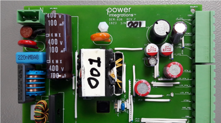
图4.40W多输出反激转换器PCB装配(顶视图)
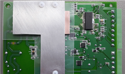
图5.40W多输出反激转换器PCB装配(底视图,带散热器)
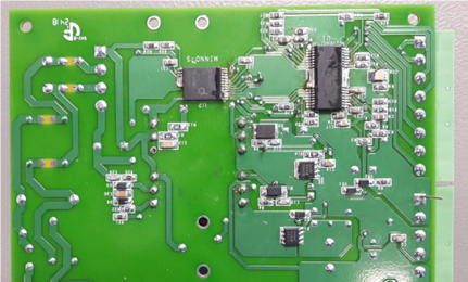
图6.40W多输出反激转换器PCB装配(底视图,不带散热器)
40W多输出反激转换器电源指标:

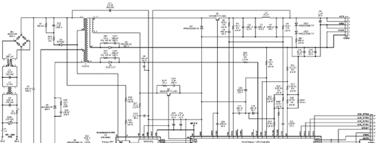
图7.40W多输出反激转换器电路图
40W多输出反激转换器材料清单:
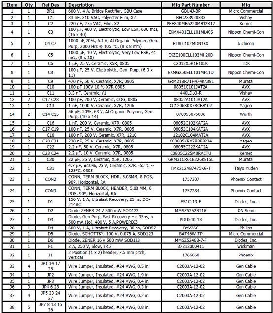
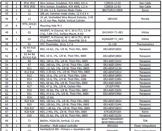
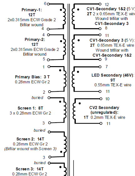
图8.40W多输出反激转换器变压器电路图
责任编辑:David
【免责声明】
1、本文内容、数据、图表等来源于网络引用或其他公开资料,版权归属原作者、原发表出处。若版权所有方对本文的引用持有异议,请联系拍明芯城(marketing@iczoom.com),本方将及时处理。
2、本文的引用仅供读者交流学习使用,不涉及商业目的。
3、本文内容仅代表作者观点,拍明芯城不对内容的准确性、可靠性或完整性提供明示或暗示的保证。读者阅读本文后做出的决定或行为,是基于自主意愿和独立判断做出的,请读者明确相关结果。
4、如需转载本方拥有版权的文章,请联系拍明芯城(marketing@iczoom.com)注明“转载原因”。未经允许私自转载拍明芯城将保留追究其法律责任的权利。
拍明芯城拥有对此声明的最终解释权。


 产品分类
产品分类




 2012- 2022 拍明芯城ICZOOM.com 版权所有 客服热线:400-693-8369 (9:00-18:00)


