TI UCC27282 120V低开关损耗半桥驱动器解决方案
 147
147
 拍明
拍明
原标题:TI UCC27282 120V低开关损耗半桥驱动器解决方案
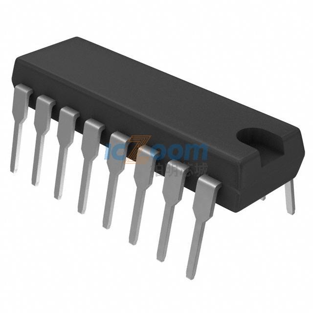
TI公司的ucc27282 120V低开关损耗和交叉导通保护的半桥驱动器,是N沟MOSFET驱动器,允许两个N-MOSFET由半桥或同步降压配置的拓扑来控制.它的3.5A峰值沉电流和2.5A峰值源电流以及低上拉和下拉电阻允许UCC27282能以最小开关损耗驱动大功率MOSFET.因为输入独立于电源电压,UCC27282可以和两个模拟和数字控制器相连.欠压锁住电压5V,输入连锁,使能/失能功能,典型传输时延为16ns,1800pF负载上升时间为12ns,下降时间为10ns,延迟匹配时间为1ns,最大启动电压120V,失能时的电流为7-μA,集成了自举电路,工作结温为–40℃到140℃.主要用在通信和商用电源,马达驱动和电动工具,辅助逆变器,半桥和全桥转换器,有源钳位正激变换器,高压同步降压转换器和D类音频放大器.本文介绍了UCC27282主要特性,功能框图,典型应用框图以及评估板UCC27282EVM-335主要特性,建立和配置图,电路图,材料清单和PCB设计图.
The UCC27282 is a robust N-channel MOSFETdriver with a maximum switch node (HS) voltagerating of 100 V. It allows for two N-channel MOSFETsto be controlled in half-bridge or synchronous buckconfiguration based topologies. Its 3.5-A peak sinkcurrent and 2.5-A peak source current along with lowpull-up and pull-down resistance allows theUCC27282 to drive large power MOSFETs withminimum switching losses during the transition of theMOSFET Miller plateau. Since the inputs areindependent of the supply voltage, UCC27282 can beused in conjunction with both analog and digital controllers.
The input pins as well as the HS pin are able totolerate significant negative voltage, which improvessystem robustness. Input interlock further improvesrobustness and system reliability in high noiseapplications. The enable and disable functionalityprovides additional system flexibility by reducingpower consumption by the driver and responds to
fault events within the system. 5-V UVLO allowssystems to operate at lower bias voltages, which isnecessary in many high frequency applications andimproves system efficiency in certain operatingmodes. Small propagation delay and delay matchingspecifications minimize the dead-time requirementwhich further improves efficiency.
Under voltage lockout (UVLO) is provided for both thehigh-side and low-side driver stages forcing theoutputs low if the VDD voltage is below the specifiedthreshold. An integrated bootstrap diode eliminatesthe need for an external discrete diode in manyapplications, which saves board space and reducessystem cost. UCC27282 is offered in a small packageenabling high density designs.
UCC27282主要特性:
• Drives Two N-Channel MOSFETs in High-SideLow-Side Configuration
• 5-V Typical Under Voltage Lockout
• Input Interlock
• Enable/Disable Functionality
• 16-ns Typical Propagation Delay
• 12-ns Rise, 10-ns Typical Fall Time With 1800-pFLoad
• 1-ns Typical Delay Matching
• Absolute Maximum Negative Voltage Handling onInputs (–5 V)
• Absolute Maximum Negative Voltage Handling onHS (–14 V)
• 3.5-A Sink, 2.5-A Source Output Currents
• Absolute Maximum Boot Voltage 120 V
• Low Current (7-μA) Consumption when Disabled
• Integrated Bootstrap Diode
• Specified from –40℃to 140℃ JunctionTemperature
UCC27282应用:
• Telecom and Merchant Power Supplies
• Motor Drives and Power Tools
• Auxiliary Inverters
• Half-Bridge and Full-Bridge Converters
• Active-Clamp Forward Converters
• High Voltage Synchronous-Buck Converters
• Class-D Audio Amplifiers
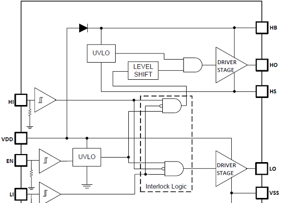
图1.UCC27282功能框图
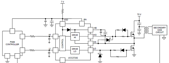
图2.UCC27282典型应用框图
评估板UCC27282EVM-335
The UCC27282EVM-335 is designed to primarily evaluate the UCC27282 performance. This driver is a100-V boot voltage, high-side, low-side driver with 3-A peak source and sink current for driving two NChannelMOSFETs. The same board can be used to evaluate other pin-to-pin compatible parts in thesupported package. The UCC27282 has low propagation delay and low propagation delay matchingbetween the high- and low-side rising and falling edges of the driver outputs for reliable timing of the gatedrive signals. The UCC27282 inputs can tolerate signals as high as 16 V regardless of the VDD voltagewhich enhances device robustness.
The UCC27282 driver includes an enable function which enables the driver outputs when pulled high, anddisables the driver into a very low standby current mode when low. The UCC27282 also includes aninterlock feature which sets both LO and HO driver outputs low when both LI and HI inputs are high at thesame time. This prevents turning on the high-side and low-side MOSFETs at the same time enhancingrobustness of the power train design.
The EVM is developed in such a way that the UCC27282 driver performance can be evaluated andcompared to data sheet parameters, or externally connected to power devices with provisions for sourceand sink gate-resistance flexibility. The UCC27282EVM-335 evaluation board uses surface-mount testpoints allowing connection to LI, HI, VDD, and HB inputs. A variety of other test points are available forprobing the UCC27282. The input bias is configured such that the VHB-VHS high-side bias can be sourced from VCC, or an external additional bias can be added to provide VHB-VHS directly. The highandlow-side driver output returns are separated on HS and GND respectively to allow evaluation of theUCC27282 HS negative voltage capabilities.
评估板UCC27282EVM-335主要特性:
• EVM for the low-voltage features of the UCC27282 gate driver
• 6-V to 16-V VCC power supply range
• TTL-compatible inputs
• PCB layout optimized for bias supply bypassing cap, gate-drive resistance selection
• Capacitive load, external gate drive resistor and diode for gate drive network evaluation
• Allows quick verification of most of the data sheet parameters
• Test points allow probing all the key pins of the UCC27282
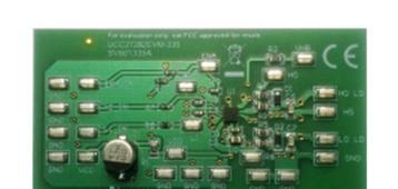
图3.评估板UCC27282EVM-335外形图
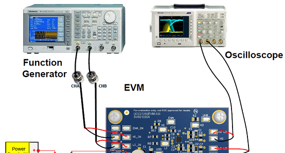
图4.评估板UCC27282EVM-335建立和配置图
评估板UCC27282EVM-335材料清单:

责任编辑:David
【免责声明】
1、本文内容、数据、图表等来源于网络引用或其他公开资料,版权归属原作者、原发表出处。若版权所有方对本文的引用持有异议,请联系拍明芯城(marketing@iczoom.com),本方将及时处理。
2、本文的引用仅供读者交流学习使用,不涉及商业目的。
3、本文内容仅代表作者观点,拍明芯城不对内容的准确性、可靠性或完整性提供明示或暗示的保证。读者阅读本文后做出的决定或行为,是基于自主意愿和独立判断做出的,请读者明确相关结果。
4、如需转载本方拥有版权的文章,请联系拍明芯城(marketing@iczoom.com)注明“转载原因”。未经允许私自转载拍明芯城将保留追究其法律责任的权利。
拍明芯城拥有对此声明的最终解释权。


 产品分类
产品分类



 2012- 2022 拍明芯城ICZOOM.com 版权所有 客服热线:400-693-8369 (9:00-18:00)


