


 产品分类
产品分类
ADI AD4111低功耗低噪音24位Σ-Δ ADC解决方案
 177
177
 拍明
拍明
原标题:ADI AD4111低功耗低噪音24位Σ-Δ ADC解决方案
ADI公司的AD4111是具有±10V和0 mA至20 mA输入和明线检测功能的低功耗 24 位 Σ-Δ ADC,集成了模拟前端(AFE),还集成主要模拟和数字的信号调理区快,为每个模拟输入通路配置成八种单独建立图,最大通路扫描速率6.2 kSPS(161 μs),嵌入的2.5V低漂移(5 ppm/℃)能隙基准电压降低了外接元件数量,单电源5V或3.3V工作,工作温度−40℃ 到 +105℃,主要用在过程控制PLC和DCS模块.本文介绍了AD4111主要特性,功能框图以及评估板EVAL-AD4111SDZ主要特性,框图,电路图,材料清单和PCB设计图.
The AD4111 is a low power, low noise, 24-bit, sigma-delta (Σ-Δ) analog-to-digital converter (ADC) that integrates an analog front end (AFE) for fully differential or single-ended, high impedance(≥1 MΩ) bipolar,±10 V voltage inputs, and 0 mA to 20 mA current inputs. The AD4111 also integrates key analog and digital signalconditioning blocks to configure eight individual setups for each analog input channel in use. The AD4111 features amaximum channel scan rate of 6.2 kSPS (161 μs) for fullysettled data.
The embedded 2.5 V, low drift (5 ppm/℃), band gap internal reference (with output reference buffer) reduces the external component count. The digital filter allows flexible settings, including simultaneous50 Hz and 60 Hz rejection at a 27.27 SPS output data rate. The user can select between the different filter settings depending on the demands of each channel in the application. The automatic channel sequencer enables the ADC to switch through eachenabled channel.
The precision performance of the AD4111 is achieved by integrating the proprietary iPassives™ technology from Analog Devices, Inc. The AD4111 is factory calibrated to achieve a high degree of specified accuracy.
The AD4111 also has the unique feature of open wire detection on the voltage inputs (patent pending) for system level diagnosticsusing a single 5 V or 3.3 V power supply. The AD4111 operates with a single power supply, making it easy to use in galvanically isolated applications. The specified operating temperature range is −40℃ to +105℃. The AD4111 is housedin a 40-lead, 6 mm × 6 mm LFCSP package.
AD4111主要特性:
24-bit ADC with integrated analog front end
Up to 6.2 kSPS per channel (161 μs per channel)
16 noise free bits at 1 kSPS per channel
85 dB rejection of 50 Hz and 60 Hz at 20 SPS per channel
±10 V inputs, 4 differential or 8 single-ended Overrange up to ±20 V ≥1 MΩ impedance
±0.06% accuracy at 25℃ Open wire detection 0 mA to 20 mA inputs,4 single-ended Overrange from −0.5 mA to +24 mA
60 Ω impedance
±0.08% accuracy at 25℃ On-chip 2.5 V reference ±0.12% accuracy at 25℃
, ±5 ppm/℃ (typical) drift Internal or external clock
Power supplies
AVDD = 3.0 V to 5.5 V
IOVDD = 2 V to 5.5 V
Total IDD = 3.9 mA
Temperature range: −40℃ to +105℃ 3-wire or 4-wire serial digital interface (Schmitt trigger on SCLK)
SPI, QSPI, MICROWIRE, and DSP compatible
AD4111应用:
Process control PLC and DCS modules

图1.AD4111功能框图
评估板EVAL-AD4111SDZ
Evaluating the AD4111 ±10 V and 0 mA to 20 mA, Analog Front End forIndustrial Automation Systems
The EVAL-AD4111SDZ evaluation kit features the AD4111,a 24-bit, 31.25 kSPS analog-to-digital converter (ADC) with a±10 V input voltage range (4 single-ended or 8 differentialchannels) with open wire detection and 4 current channelsoperating from 0 mA to 20 mA. All channels have on-board overvoltage and overcurrent protection. The EVAL-AD4111SDZ board includes voltage reference, power, and data insulation and can be connected to the Analog Devices, Inc., SDP-B system demonstration platform (EVAL-
SDP-CB1Z). The SDP-B board provides connection to a PC viaUSB port and can provide power for the EVAL-AD4111SDZboard from the PC USB port.
The AD411X Eval+ evaluation software configures the AD4111device functionality and provides open wire detection, dc timedomain analysis in the form of waveform graphs, histograms,and associated noise analysis for ADC performance evaluation.
Full specifications for the AD4111 are available in the productdata sheet, which must be consulted in conjunction with thisuser guide when working with this evaluation board.
评估板EVAL-AD4111SDZ主要特性:
Fully featured evaluation board for the AD4111
PC control in conjunction with Analog Devices, Inc., SDP-B
system demonstration platform (EVAL-SDP-CB1Z)
PC software for control and data analysis (time domain)
评估板EVAL-AD4111SDZ包括:
EVAL-AD4111SDZ evaluation board
Required software: AD411X Eval+
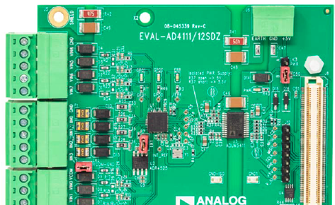
图2.评估板EVAL-AD4111SDZ外形图

图3. 评估板EVAL-AD4111SDZ框图

图4. 评估板EVAL-AD4111SDZ硬件配置图

图5.评估板EVAL-AD4111SDZ电路图:AD4111

图6.评估板EVAL-AD4111SDZ电路图:电压输入前端

图7.评估板EVAL-AD4111SDZ电路图:电流输入前端

图8.评估板EVAL-AD4111SDZ电路图:SDP连接器

图9.评估板EVAL-AD4111SDZ电路图:隔离和电源
评估板EVAL-AD4111SDZ材料清单:


责任编辑:HanFeng
【免责声明】
1、本文内容、数据、图表等来源于网络引用或其他公开资料,版权归属原作者、原发表出处。若版权所有方对本文的引用持有异议,请联系拍明芯城(marketing@iczoom.com),本方将及时处理。
2、本文的引用仅供读者交流学习使用,不涉及商业目的。
3、本文内容仅代表作者观点,拍明芯城不对内容的准确性、可靠性或完整性提供明示或暗示的保证。读者阅读本文后做出的决定或行为,是基于自主意愿和独立判断做出的,请读者明确相关结果。
4、如需转载本方拥有版权的文章,请联系拍明芯城(marketing@iczoom.com)注明“转载原因”。未经允许私自转载拍明芯城将保留追究其法律责任的权利。
拍明芯城拥有对此声明的最终解释权。
相关资讯
:
基于MC33771主控芯片的新能源锂电池管理系统解决方案

AMIC110 32位Sitara ARM MCU开发方案

基于AMIC110多协议可编程工业通信处理器的32位Sitara ARM MCU开发方案

基于展讯SC9820超低成本LTE芯片平台的儿童智能手表解决方案

基于TI公司的AM437x双照相机参考设计

基于MTK6580芯片的W2智能手表解决方案


 2012- 2022 拍明芯城ICZOOM.com 版权所有 客服热线:400-693-8369 (9:00-18:00)


