


 产品分类
产品分类
Microsemi MSCSICSP6(REF3)高温SiC MOSFET解决方案
 154
154
 拍明
拍明
原标题:Microsemi MSCSICSP6(REF3)高温SiC MOSFET解决方案
Microsemi公司的MSCSICSP6/REF3是新一代SiC MOSFETS和SiC SBD,具有零反向恢复电荷,从而提升系统效率,具有高热导率,是通常硅器件的2.5X,从而降低尺寸和提高工作温度以及功率密度等优势,满足AEC- Q101规范,主要用在工业如马达驱动,焊接,UPS和SMPS,汽车如EV电池充电器,动力总成,智能能源如PV逆变器,风力涡轮机,医疗如MRI和X光电源,军用国防和航空航天,以及通信市场.本文介绍了MSCSICSP6/REF3主要特性,以及SP6LISiC模块参考设计主要特性,电路图和材料清单.
Silicon Carbide (SiC) semiconductors are an innovative newoption for power electronic designers looking for improvedsystem efficiency, smaller form factor and higher operating temperature in products covering industrial, medical,mil-aerospace, aviation, and communcation marketsegments. Microsemi’s next-generation SiC MOSFETS andSiC SBDs are designed with higher repetitive unclampedinductive switching (UIS) capability at rated current,with no degradation or failures. The new SiC MOSFETsmaintain high UIS capability at approximately 10-15 Joulesper square centimeter (J/cm2) and robust short circuitprotection at 3-5 microseconds. The company’s SiC SBDsare designed with balanced surge current,forward voltage, thermal resistance and thermal capacitance ratings atlow reverse current for lower switching loss. In addition,its SiC MOSFET and SiC SBD die can paired together foruse in modules. SiC MOSFET and SiC SBD products fromMicrosemi will be qualified to the AEC-Q101 standard.
MSCSICSP6/REF3主要特性:
Extremely Low Switching Losses
• Zero reverse recovery charge improvessystem efficiency
High Power Density
• Smaller footprint device reduces system sizeand weight
High Thermal Conductivity
• 2.5x more thermally conductive than silicon
Reduced Sink Requirements
• Results in lower cost and smaller size
High Temperature Operation
• Increased power density and improved
Reliability
Power Module Advantages
• High-speed switching
• Low switching losses
• Low input capacitance
• High power density
• Low profile packages
• Minimum parasiticinductance
• Lower system cost
• Standard & custom modules
• Choice of Si/SiC devices
Silicon Carbide (SiC) is the ideal technology for higher switchingfrequency, higher efficiency, and higher power (>650 V)applications. Target markets and applications include:
• Industrial—motor drives, welding, UPS, SMPS,induction heating
• Transportation/automotive—EV battery charger,onboard chargers, hybrid electric vehicle (HEV)/electricvehicle (EV) powertrain, DC–DC converter, energy recovery
• Smart energy—PV inverter, wind turbine
• Medical—MRI power supply, X-ray power supply
• Commercial aviation—actuation, air conditioning,power distribution
• Defense—motor drives, auxiliarypower supplies, integrated vehicle systems
SiC MOSFET and SiCSchottky Barrier Diode product linesfrom Microsemi increase your system efficiency over siliconMOSFET and IGBT solutions while lowering your total cost ofownership by enabling downsized systems and smaller/lowercost cooling.

图1. MSCSICSP6/REF3外形图
SP6LISiC模块参考设计
This reference design provides an example of a highly isolated SiC MOSFET dual-gate driver for the SP6LISiC phase leg modules. It can be configured by switches to drive in a half-bridge configuration with onlyone side on at any time and with dead time protection. It can also be configured to provide concurrentdrive, if necessary. This design is intended for use with MicrosemiSiC SP6LI modules. The dead time andgate drive resistance are adjusted by the user to match the requirements of the application. Optionaldead time protection and optional desaturation protection makes device evaluation easier while lowering the risk of damaging parts.
This design is offered as an engineering tool for the evaluation of Microsemi SP6LI SiC modules in alaboratory environment. It has not been tested at voltage across the insulation boundaries. It is theresponsibility of the engineer to use the proper safety equipment and procedures. Refer to theappropriate UL or IEC standards for guidance on insulation and creepage requirements.

图2. SP6LISiC模块参考设计外形图

图3.带半桥的SP6LISiC模块参考设计框图
This reference design is optimized to drive SP6LI SiC MOSFET devices at high speeds with desaturationprotection. It is a base design that can be simplified depending upon the individual systemrequirements.
SP6LISiC模块参考设计主要特性:
Requires only a 12 V power input
–5 V, 20 V output gate drive, jumper selectable to–5 V, 18 V
Includes an example of temperature monitoring
Galvanic isolation of more than 2000 V on both gate drivers1
Capable of 16 W of gate drive power/side
Peak gate current of up to 30 A
Maximum output current of approximately 150 A due to limitations of the trace
Maximum switching frequency greater than 400 kHz2
Single-ended or RS485/RS422 differential input gate control
Shoot through(short-circuit) protection
±100 kV/μs capability
Programmable dead time protection
Fault signaling
Under voltage lockout protection
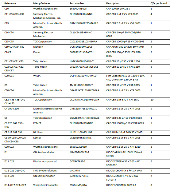
材料清单:


责任编辑:HanFeng
【免责声明】
1、本文内容、数据、图表等来源于网络引用或其他公开资料,版权归属原作者、原发表出处。若版权所有方对本文的引用持有异议,请联系拍明芯城(marketing@iczoom.com),本方将及时处理。
2、本文的引用仅供读者交流学习使用,不涉及商业目的。
3、本文内容仅代表作者观点,拍明芯城不对内容的准确性、可靠性或完整性提供明示或暗示的保证。读者阅读本文后做出的决定或行为,是基于自主意愿和独立判断做出的,请读者明确相关结果。
4、如需转载本方拥有版权的文章,请联系拍明芯城(marketing@iczoom.com)注明“转载原因”。未经允许私自转载拍明芯城将保留追究其法律责任的权利。
拍明芯城拥有对此声明的最终解释权。
相关资讯
:
基于MC33771主控芯片的新能源锂电池管理系统解决方案

AMIC110 32位Sitara ARM MCU开发方案

基于AMIC110多协议可编程工业通信处理器的32位Sitara ARM MCU开发方案

基于展讯SC9820超低成本LTE芯片平台的儿童智能手表解决方案

基于TI公司的AM437x双照相机参考设计

基于MTK6580芯片的W2智能手表解决方案


 2012- 2022 拍明芯城ICZOOM.com 版权所有 客服热线:400-693-8369 (9:00-18:00)


