Lattice数据速率1.65Gbps的HDMI接口解决方案
 20
20
 拍明芯城
拍明芯城
原标题:Lattice数据速率1.65Gbps的HDMI接口解决方案
lattice公司的HDMI接口板支持基于SERDES的DVI和HDMI接口,数据速率高达1.65Gbps,共享TMDS编码器和译码器,对于DVI和HDMI数据
HDMI is an industry-supported, all-digital audio/video interface for transmitting both uncompressed digital video and multi-channel audio over a single connector and cable that replaces various cables behind the home entertainment center. HDMI can carry eight channels of 192KHz, 24-bit uncompressed audio, or any flavor of compressed audio format such as Dolby or DTS. HDMI has the capacity to support existing high-definition video formats such as 720p, 1080i, and 1080p. Because HDMI is electrically compatible with the DVI signal, no signal conversion is required, nor is there a loss of video quality when a DVI-to-HDMI adapter is used.
HDMI接口板主要特性:
SERDES-based DVI and HDMI interface supports data rate up to 1.65Gbps
Shared TMDS Encoder and Decoder for both DVI and HDMI data
Supports arbitrary HSYNC/VSYNC polarity
PCS Embedded Word Alignment and FPGA FIFO-based Channel Alignment
Multi-Channel Alignment exceeds the inter-channel skew requirements of DVI and HDMI Specifications
Emulated Extended Display Identification Data (EDID) support for DVI
The LatticeECP3 Versa Development Kit is the industry’s lowest cost design platform for building leading edge systems in a variety of markets such as industrial networking, industrial automation, computing, medical equipment, defense, and consumer electronics. It brings high-end innovations -- configurable SERDES, cascadable DSP slices, and high-speed DDR3 memory within the reach of mainstream designers in an easy to use environment. The Versa Kit empowers designers to build both PCI Express and Gigabit Ethernet based systems. The Kit offers free design tools, readymade demos, reference designs, a versatile evaluation board, and a serial programming cable. The evaluation board features an LFE3-35EA-8FN484C FPGA device, 64 Mbit SPI Flash, 1Gbit DDR3 memory, expansion headers, several LEDs, and user switches. It contains a PCI Express x1 (Half-length form-factor), two RJ45, and 4 SMA interfaces.

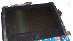
图1.HDMI子板外形图
HDMI子板主要特性:
• Supports two different HDMI/DVI input paths, with or without the cable equalizer
• Supports HDMI/DVI output with TMDS level shifter
• TOSLINK fiber optic receiving module for S/PDIF audio input
• Headers for HPD, CEC controls and the EDID signals
• ESD protection devices for both HDMI/DVI inputs and HDMI/DVI outputs

图2.HDMI子板方框图

图3.安装在LatticeECP3 视频协议板的HDMI子板
责任编辑:HanFeng
【免责声明】
1、本文内容、数据、图表等来源于网络引用或其他公开资料,版权归属原作者、原发表出处。若版权所有方对本文的引用持有异议,请联系拍明芯城(marketing@iczoom.com),本方将及时处理。
2、本文的引用仅供读者交流学习使用,不涉及商业目的。
3、本文内容仅代表作者观点,拍明芯城不对内容的准确性、可靠性或完整性提供明示或暗示的保证。读者阅读本文后做出的决定或行为,是基于自主意愿和独立判断做出的,请读者明确相关结果。
4、如需转载本方拥有版权的文章,请联系拍明芯城(marketing@iczoom.com)注明“转载原因”。未经允许私自转载拍明芯城将保留追究其法律责任的权利。
拍明芯城拥有对此声明的最终解释权。


 产品分类
产品分类



 2012- 2022 拍明芯城ICZOOM.com 版权所有 客服热线:400-693-8369 (9:00-18:00)


