


 产品分类
产品分类
SiC and GaN Semiconductors Deliver for Power Electronics
 197
197
 Majeed Ahmad
原标题:SiC and GaN Semiconductors Deliver for Power Electronics
Silicon carbide (SiC) and gallium nitride (GaN) are becoming the wide bandgap (WBG) technology of choice for the next generation power designs in electric vehicles, industrial power supplies, and solar power systems. Let’s look for a minute at what’s happening and why WBG technologies may provide an alternate way forward while looking at some cutting edge WBG solutions that will get us there.
From hybrid and electric vehicles to data centers and military power electronics, SiC and GaN semiconductor materials have emerged as a viable option to improve power conversion and energy savings in high voltage power electronics.
For example, powertrain inverters in electric vehicles (EVs) have long relied upon silicon-based IGBTs, but designers of EVs are increasingly using SiC MOSFETs that operate at higher frequencies and are suitable for high breakdown voltage applications. As a result, SiC devices are enjoying strong growth in hybrid and electric vehicles with the availability of SiC Schottky barrier diodes (SBDs), SiC MOSFETs, SiC junction gate field-effect transistors (JFETs) and other SiC discretes. The next logical step we can expect is the release of full SiC modules.
For their part, GaN semiconductors promise lower cost, they are easier to manufacture as compared to SiC wafers, and they are catching up with SiC volumes. Along with automotive designs like inverters, GaN devices are now also becoming popular in DC-DC converters in the datacenter, high voltage power supplies, and military power electronics.
SiC: Higher power density and reliability
SiC materials feature a wide bandgap of 2.86 electronvolts (eV)1, so they have a higher thermal conductivity compared to silicon, at 1.11 eVs. As such, they can drive high voltages for high-power applications. Their ability to offer higher power density, durability and reliability makes them suitable for power conversion systems for vehicle electrification, solar inverters, and other high-power applications.
For example, the E-Series of SiC MOSFETs from Wolfspeed, a Cree company, is optimized for EV battery chargers and high voltage DC/DC converters. The E-Series is based on Wolfspeed’s third-generation rugged planar technology and is featured in the company’s 6.6 kilowatt (kW) bidirectional on-board charger reference design.
Wolfspeed positions the E-Series SiC MOSFETs as having the industry’s lowest switching losses and highest figure of merit (FOM). Indeed, it does have an RDSon as low as 65 milliohms (mΩ) so the FOM, which takes into account the electrical power losses and thermal limitations for WBG power devices, may well be at or near the top at the time of this writing.
Moreover, for solar power systems operating in extremely harsh environments, these SiC devices comply to the HV-H3TRB rating. They complied while at 80 percent of the rated blocking voltage in an environmental chamber at a constant 85⁰C ambient temperature with 85 percent relative humidity.
Rohm Semiconductor has also made available the third-generation of its SiC SBDs in a variety of current ratings and packages. The SBDs significantly improve the Vf characteristics and provide higher surge current resistance while lowering the leakage. As a result, the devices can have a lower switching loss than silicon fast recovery diodes (SiFRDs).
Additionally, Rohm has released power modules that integrate SiC MOSFETs and SBDs in an industrial standard package (Figure 1).

Figure 1: Much reduced RDS(ON) is a key reason power modules using third-generation SiC MOSFETs have lower switching losses. (Image source: Rohm Semiconductor)
The full-SiC half-bridge power modules have switching losses significantly lower than conventional IGBT modules and allow high-frequency operation above 100 kHz.
GaN: Smaller and faster than silicon
GaN offers an even higher bandgap of 3.4 eVs and twice the electron mobility compared to silicon. Furthermore, the current-collapse-free characteristics of GaN devices lower the size and improve the efficiency of power conversion systems.
Take for example EPC’s EPC2206 device (Figure 2). Part of the eGaN® FET family, the EPC2206 is targeted at vehicles using a 48 volt power distribution bus to facilitate features such as electric start-stop, electric steering, electronic suspension, and variable speed air conditioning. EPC2206 eGaN FETs are supplied only in passivated die form with solder bars. The die size is 6.05 millimeters (mm) x 2.3 mm.
.png")
Figure 2: EPC’s EPC2206 eGaN FETs are supplied only in passivated die form with solder bars. The die size is 6.05 mm x 2.3 mm. (Image source: EPC)
EPC’s EPC2100 half-bridge GaN transistors are also part of the eGaN FET family (Figure 3, top). To simplify the integration of power FETs into converter designs, EPC has also made available the EPC9036 development board (Figure 3, bottom).
. It measures 6.05 mm x 2.3 mm. Two of them are placed in parallel on the EPC9059 development board (bottom). (Image source: Digi-Key Electronics).png")
Figure 3: The EPC2100 half-bridge GaN transistor comes in passivated die form with solder bumps (top). It measures 6.05 mm x 2.3 mm. Two of them are placed in parallel on the EPC9059 development board (bottom). (Image source: Digi-Key Electronics)
The EPC9036 development board has two 30 volt EPC2100 eGaN ICs in parallel with a single on-board gate drive for higher output currents. It has all critical components and layout for optimal switching performance.
Then there is Transphorm, which launched the first automotive AEC-Q101 qualified GaN transistor in 2017. According to Transphorm, its high voltage GaN FETs give you ample thermal headroom when developing a power system. Its TP65H035WSQA is its Gen III AEC-Q101-qualified GaN device and has expanded the FET’s thermal limits to 175°C. This is 25°C greater than AEC-Q101-qualified high voltage silicon MOSFETs.
The above solutions demonstrate that SiC and GaN power devices have fully emerged commercially. As they continue to address critical design challenges in key application areas, volume and usability will increase, which will help bring them closer to their silicon counterparts in terms of drop-in replacement.
责任编辑:David
【免责声明】
1、本文内容、数据、图表等来源于网络引用或其他公开资料,版权归属原作者、原发表出处。若版权所有方对本文的引用持有异议,请联系拍明芯城(marketing@iczoom.com),本方将及时处理。
2、本文的引用仅供读者交流学习使用,不涉及商业目的。
3、本文内容仅代表作者观点,拍明芯城不对内容的准确性、可靠性或完整性提供明示或暗示的保证。读者阅读本文后做出的决定或行为,是基于自主意愿和独立判断做出的,请读者明确相关结果。
4、如需转载本方拥有版权的文章,请联系拍明芯城(marketing@iczoom.com)注明“转载原因”。未经允许私自转载拍明芯城将保留追究其法律责任的权利。
拍明芯城拥有对此声明的最终解释权。
相关资讯
:
BAT剑指科大讯飞,能否让其重蹈Nuance覆辙?

三星在中国一面撤资,一面增资是为何?
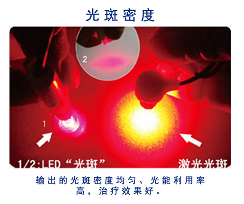
半导体激光治疗仪是骗局吗?

2016全球十大电子元器件分销商排行榜

2016年10大全球电子元器件代理商排行一览表
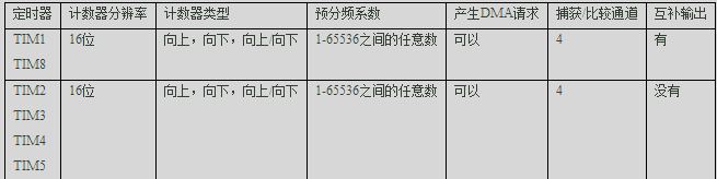
STM32学习笔记:通用定时器基本定时功能


 2012- 2022 拍明芯城ICZOOM.com 版权所有 客服热线:400-693-8369 (9:00-18:00)


