


 产品分类
产品分类
TI ADS5294 80MSPS 8路医学图像解决方案
 97
97
 拍明
拍明
原标题:TI ADS5294 80MSPS 8路医学图像解决方案
TI公司的ADS5294是80MSPS/14位 8路ADC,具有低功耗,高SNR和低SFDR,以及连续过载恢复,适用于高性能系统设计. ADS5294具有数乁信号处理核,包括数字滤波器模块, 可编程数字增益0 dB到12 dB,内部和外接基准电压,1.8V工作电压,主要用在超声图像,通信设备和多路数据采集.本文介绍了ADS5294主要特性,方框图, 模拟输入模型和电路,评估模块测试图以及评估模块电路图,材料清单和PCB布局图.
Using CMOS process technology and innovative circuit techniques, the ADS5294 is a low power 80MSPS 8-Channel ADC. Low power consumption, high SNR, low SFDR, and consistent overload recovery allow users to design high performance systems.
The ADS5294 has a digital processing block that integrates several commonly used digital functions for improving system performance. It includes a digital filter module that has built-in decimation filters (with low-pass, high-pass and band-pass characteristics).
The decimation rate is also programmable (by 2, by , or by 8). This makes it useful for narrow-band applications, where the filters can be used conveniently to improve SNR and knock-off harmonics, while at the same time reducing the output data rate. The device includes an averaging mode where two channels (or even four channels) can be averaged to improve SNR.
Serial LVDS outputs reduce the number of interface lines and enable the highest system integration. The digital data from each channel ADC can be output over one or two wires of LVDS output lines depending on the ADC sampling rate. This 2-wire interface helps keep the serial data rate low, allowing low cost FPGA based receivers to be used even at high sample rate. The ADC resolution can be programmed to 12 bit or 14 bit through register. A very unique feature is the programmable mapping module that allows flexible mapping between the input channels and the LVDS output pins. This helps greatly reduce the complexity of LVDS output routing and can potentially result in cheaper system boards by reducing the number of PCB layers.
The device integrates an internal reference trimmed to accurately match across devices. Best performance is expected to be achieved through the internal reference mode. The device can be driven with external references as well. The device is available in a 12 mm × 12 mm 80-pin QFP. It is specified over a –40°C to 85°C operating temperature range. ADS5294 is completely pin-to-pin and register compatible to ADS5292 QFP. It is specified over a –40°C to 85°C operating temperature range. ADS5294 is completely pin-to-pin and register compatible to ADS5292.
ADS5294主要特性:
Maximum Sample Rate: 80 MSPS/14-Bit
High Signal-to-Noise Ratio
75.5-dBFS SNR at 5 MHz/80 MSPS
78.2-dBFS SNR at 5 MHz/80 MSPS and Decimation Filter Enabled
84-dBc SFDR at 5 MHz/80 MSPS
Low Power Consumption
58 mW/CH at 50 MSPS
77 mW/CH at 80 MSPS (2 LVDS Wire Per Channel)
Digital Processing Block
Programmable FIR Decimation Filter and Oversampling to
Minimize Harmonic Interference
Programmable IIR High Pass Filter to Minimize DC Offset
Programmable Digital Gain: 0 dB to 12 dB
2- or 4- Channel Averaging
Flexible Serialized LVDS Outputs:
One or Two Wires of LVDS Output Lines per Channel
Depending on ADC Sampling Rate
Programmable Mapping Between ADC Input Channels and
LVDS Output Pins-Eases Board Design
Variety of Test Patterns to Verify Data Capture
by FPGA/Receiver
Internal and External References
1.8V Operation for Low Power Consumption
Low-Frequency Noise Suppression
ADS5294应用:
Ultrasound Imaging
Communication Applications
Multi-channel Data Acquisition
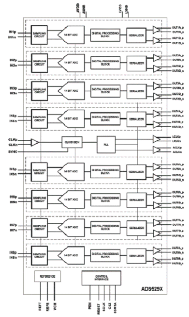
图1. ADS5294方框图
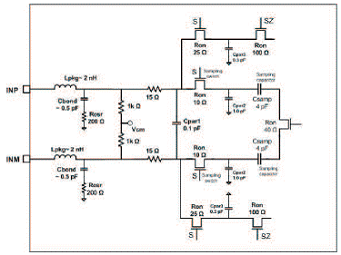
图2. ADS5294模拟输入模型
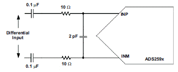
图3. ADS5294模拟输入驱动电路
ADS5294评估模块
This user’s guide gives a general overview of the evaluation module (EVM) and provides a general description of the features and functions to be considered while using this module. This manual is applicable to the ADS5294 analog-to-digital converters (ADC), which collectively are referred to as ADS529x. Use this document in combination with the respective ADC data sheet. The ADS529xEVM provides a platform for evaluating the ADC under various signal, clock, reference, and power supply conditions.
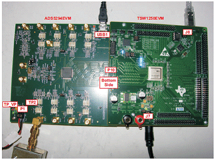
图4.ADS5294 EVM和TSW1250EVM硬件连接图
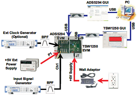
图5.ADS5294评估测试图
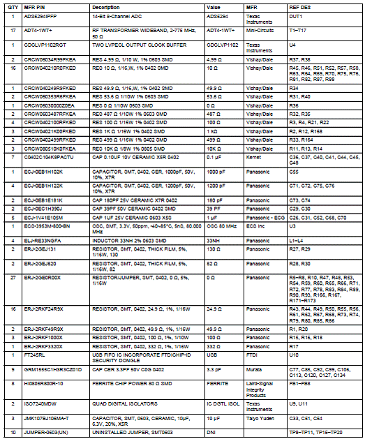
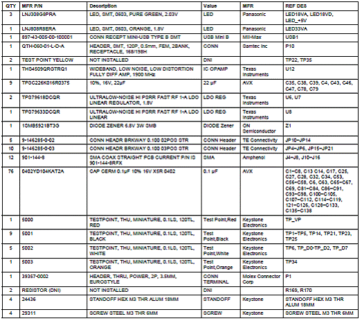
ADS5294 EVM材料清单(BOM):
责任编辑:HanFeng
【免责声明】
1、本文内容、数据、图表等来源于网络引用或其他公开资料,版权归属原作者、原发表出处。若版权所有方对本文的引用持有异议,请联系拍明芯城(marketing@iczoom.com),本方将及时处理。
2、本文的引用仅供读者交流学习使用,不涉及商业目的。
3、本文内容仅代表作者观点,拍明芯城不对内容的准确性、可靠性或完整性提供明示或暗示的保证。读者阅读本文后做出的决定或行为,是基于自主意愿和独立判断做出的,请读者明确相关结果。
4、如需转载本方拥有版权的文章,请联系拍明芯城(marketing@iczoom.com)注明“转载原因”。未经允许私自转载拍明芯城将保留追究其法律责任的权利。
拍明芯城拥有对此声明的最终解释权。
相关资讯
:
基于MC33771主控芯片的新能源锂电池管理系统解决方案

AMIC110 32位Sitara ARM MCU开发方案

基于AMIC110多协议可编程工业通信处理器的32位Sitara ARM MCU开发方案

基于展讯SC9820超低成本LTE芯片平台的儿童智能手表解决方案

基于TI公司的AM437x双照相机参考设计

基于MTK6580芯片的W2智能手表解决方案


 2012- 2022 拍明芯城ICZOOM.com 版权所有 客服热线:400-693-8369 (9:00-18:00)


