


 产品分类
产品分类
Avnet ADI ADP1850 Xilinx 7系列FPGA电源解决方案
 121
121
 拍明
拍明
原标题:Avnet ADI ADP1850 Xilinx 7系列FPGA电源解决方案
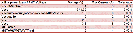
Avnet公司的ADI电源模块是采用ADI公司的ADP1850 器件,专为Xilinx 公司的7系列FPGA提供电源,12V 电压输入,四个双路ADP1850器件提供8路稳压输出:3.3V/8A,2.5V/8A,2.0V/2A,1.8V/6A,1.5V或1.35V /4A,1.2V/4A和两路1.0V/6A.输出误差在3%或5%.本文介绍了ADI电源模块主要指标和特性,方框图,电路图,材料清单和PCB布局图.
The Analog Devices Power Module provides a proven robust design for powering Xilinx 7 series devices. Designed to meet the tolerance and sequencing guidelines set forth by Xilinx, the Analog Devices Power Module provides a highly optimized controller based design utilizing the ADP1850 dual output synchronous buck controller. The device operates in current mode for improved transient response and uses valley current sensing for enhanced noise immunity. The ADP1850 is ideal in system applications requiring multiple output voltages: the ADP1850 includes a synchronization feature to eliminate beat frequencies between switching devices; provides accurate tracking capability between supplies and includes precision enable for simple, robust sequencing. The ADP1850 provides high speed, high peak current drive capability with dead-time optimization to enable energy efficient power conversion. For low load operation, the device can be configured to operate in power saving mode (PSM) by skipping pulses and reducing switching losses to improve the energy efficiency at light load and standby conditions.
Additional flexibility is provided by external programmability of loop compensation, soft start, frequency setting, power saving mode, current limit and current sense gain can all be programmed using external components.
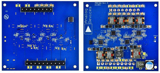
图1.ADI电源模块外形图
ADI电源模块主要指标:
ADI电源模块主要特性:
12 V input
Eight regulated outputs (4 dual output ADP1850 devices)
3.3 V @ 8 A output, 5% tolerance
2.5 V @ 8 A output, 5% tolerance
2.0 V @ 2 A output, 3% tolerance
1.8 V @ 6 A output, 5% tolerance
1.5 V/1.35 V @ 4 A jumper selectable output, 5% tolerance
1.2 V @ 4 A output, 2.5% tolerance
1.0 V @ 6 A output, 3% tolerance
Second 1.0 V @ 6 A output, 3% tolerance
Remote sense for greater regulation accuracy at the load on all outputs
Meets recommended start up sequencing for Xilinx 7 series devices
Vccint -> Vccaux -> Vccaux_io -> Vcco
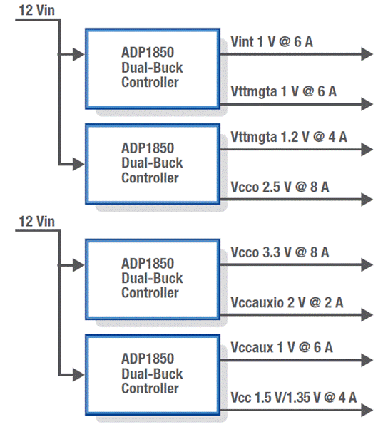
图2.ADI电源模块框图
责任编辑:HanFeng
【免责声明】
1、本文内容、数据、图表等来源于网络引用或其他公开资料,版权归属原作者、原发表出处。若版权所有方对本文的引用持有异议,请联系拍明芯城(marketing@iczoom.com),本方将及时处理。
2、本文的引用仅供读者交流学习使用,不涉及商业目的。
3、本文内容仅代表作者观点,拍明芯城不对内容的准确性、可靠性或完整性提供明示或暗示的保证。读者阅读本文后做出的决定或行为,是基于自主意愿和独立判断做出的,请读者明确相关结果。
4、如需转载本方拥有版权的文章,请联系拍明芯城(marketing@iczoom.com)注明“转载原因”。未经允许私自转载拍明芯城将保留追究其法律责任的权利。
拍明芯城拥有对此声明的最终解释权。
相关资讯
:
基于MC33771主控芯片的新能源锂电池管理系统解决方案

AMIC110 32位Sitara ARM MCU开发方案

基于AMIC110多协议可编程工业通信处理器的32位Sitara ARM MCU开发方案

基于展讯SC9820超低成本LTE芯片平台的儿童智能手表解决方案

基于TI公司的AM437x双照相机参考设计

基于MTK6580芯片的W2智能手表解决方案


 2012- 2022 拍明芯城ICZOOM.com 版权所有 客服热线:400-693-8369 (9:00-18:00)


