


 产品分类
产品分类
MAXIM 基于MAX16834实现112W高亮串型LED驱动方案
 132
132
 拍明
拍明
原标题:MAXIM 基于MAX16834实现112W高亮串型LED驱动方案
MAXIM公司的MAX16834是一款采用BOOST、BOOST-BUCK及高边BUCK拓扑结构的电流模式高亮 LED驱动器。该芯片不但具有驱动一个功率N沟道MOSFET来驱动电源,而且还可以通过一个N沟道PWM开关实现LED的亮度调节。MAX16834集成了具有宽范围亮度调节所需要的恒频高亮度内嵌模块。该芯片具有外部使能引脚、内嵌振荡器、过温故障保护、开/短路保护及过压保护模块。本文通过介绍采用MAX16834的112W高亮LED参考设计,给出设计概述、电路设计板图、电路原理图、电子元器件列表、电路板各测试点波形图等,并给出设计中的设计注意要点,以便工程师快速实现设计。
This reference design uses the MAX16834 to create a high-powered LED driver for a very long string(s) of LEDs. The LED current is adjustable with a potentiometer, and can be set as high as 1.5A into as many as 20 LEDs (75V total). For long life, ceramic capacitors are used for both input and output decoupling.
This is a reference design for a 112.5W boost LED driver that uses the MAX16834 for long strings of LEDs. These long LED strings are commonly found in streetlights and parking garage lights.
Input voltage: 24VDC ±5% (at 1.49A)
VLED configuration: Two parallel strings. Each string consists of 19 WLEDs and a 5Ω resistor for current balancing. Current is 750mA per sting for a total of 1.5A into 75V.
Dimming: 50µs (min) on-pulse for up to a 200:1 dimming ratio with a 100Hz dimming frequency
Note: this design has been built and tested. However, detailed testing has not occurred and there may be nuances that have yet to be discovered.
More detailed image (PDF, 7.6MB)
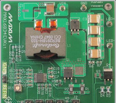
Figure 1. The LED driver board.
More detailed image (PDF, 290kB)
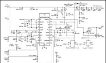
Figure 2. Schematic of the LED driver.
Figure 3. Layout of the LED driver.

More detailed image (PDF, 1.7MB)
Figure 4. Bill of materials.
More detailed image (PDF, 1.3MB)
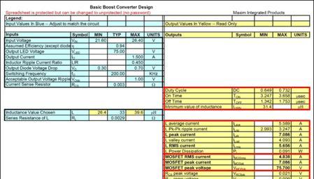
Figure 5. Design spreadsheet provides peak and RMS currents in the MOSFET and inductor. To get the spreadsheet for use in your design, contact your local Maxim sales office.
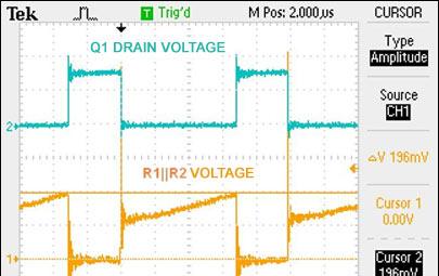
Figure 6. Switching MOSFET voltage and current-sense resistor voltage.

Figure 7. Output voltage (AC coupled) and switching MOSFET current-sense resistor voltage.
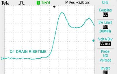
Figure 8. Drain voltage risetime.
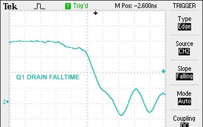
Figure 9. Drain voltage falltime.
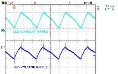
Figure 10. LED voltage (AC coupled) and current ripple.

Figure 11. LED voltage (AC coupled) and MOSFET current-sense voltage.
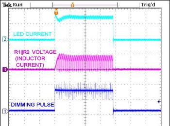
Figure 12. Dimming pulse of ~150µs.
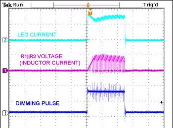
Figure 13. Dimming pulse of ~50µs.
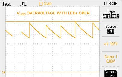
Figure 14. OVP with open LED string.
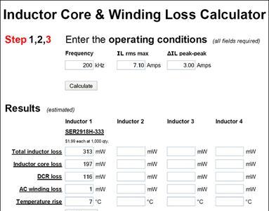
Figure 15. Predicted inductor temperature rise. The calculator is available from Coilcraft® design support tools.
Circuit Description
Overview
This reference design is for a high-voltage boost current source for very long strings of LEDs. Applications that use long LED strings include, but are not limited to, streetlights and parking garage lights. Long LED strings can be a very cost-effective way to drive LEDs. Also, since the LEDs will have exactly the same current, brightness variations are nicely controlled. This design has a 24V input, up to a 75V LED output, and drives 1.5A through the LED string (or strings, if paralleled). The measured input power is 115.49W and the output power is 111.6W for an efficiency of about 96.6%.
PCB
The printed circuit board (PCB) is a general-purpose two-layer board for MAX16834 boost designs (Figures 1 and 3). Some PCB features are optional and not populated in the tested design; they are indicated on the schematic (Figure 2) as "no-pop." The layout uses a ground island below the IC that is single point connected to the power ground for low-noise operation. The design also uses the TSSOP version of the IC, since many streetlight manufacturers will not have the equipment to properly solder the alternate package, a TQFN. Figure 4 shows a Bill of Materials for this design.
Topology
This design is for a 200kHz continuous-boost regulator. In Figure 5 the spreadsheet printout shows the RMS and peak currents in the MOSFET and inductor. Continuous designs have the advantage of lower MOSFET and inductor currents. However, since current flows through the output diode (D2) when the MOSFET (Q1) turns on, the reverse recovery losses in the output diode result in higher dissipation and possibly higher turn-off noise. Inspecting the circuit waveforms in Figure 6, you can see that the on-time of the MOSFET is about 3.4µs and the off-time is about 1.5µs for a 69% duty cycle. Once the MOSFET turns off, the drain voltage rises to the output voltage plus a Schottky diode drop.
MOSFET Drive
Because of the continuous design, the peak MOSFET and inductor currents are less than what they would be with a discontinuous design. However, since there is current through the MOSFET during turn-on and turn-off, the MOSFET experiences switching losses during both transitions. The MAX16834 drives the MOSFET hard enough for the switch to turn on in about 5ns and turn off in 10ns (Figures 8 and 9), thus keeping the temperature rise low. If EMI becomes a problem, change the series resistor, R5, on the MOSFET gate to adjust the switching times. If this action causes too much power dissipation, place a second MOSFET, Q2, in parallel with Q1 to reduce the temperature rise.
Output Capacitance
For the input and output capacitance, the driver uses ceramic capacitors. Ceramic capacitors are durable and small but have limited capacitance, especially with a 200V rating which this design needs. In Figure 5, the design spreadsheet indicates that the driver needs 5.4µF to meet the desired output ripple voltage; to reduce cost and space, this circuit uses four 1.2µF capacitors (4.8µF in total). Consequently, the output voltage switching ripple is 2.88V (Figures 10 and 11), resulting in a current ripple of 182mA. This is 12% of the output current, somewhat higher than the target of 10% but still acceptable.
Dimming
The MAX16834 is well suited for dimming. When the PWMDIM (pin 12) goes low, three things happen. First, the gate drive (NDRV, pin 15) of the switching MOSFET, Q1, goes low. This prevents the delivery of additional energy to the LED string. Secondly, the gate drive (DIMOUT, pin 20) of the dimming MOSFET, Q4, goes low, immediately curtailing the LED string current and holding the voltage on the output capacitors constant. Finally, to keep the compensation capacitance at a steady-state voltage, the COMP (pin 5) goes to high impedance. This ensures that the IC will start at the correct duty cycle immediately after PWMDIM returns high. Each of these actions allows for short PWM on-times, and thus, fairly high dimming ratios.
The main limitation to short on-times is the charge-up time of the inductor. Looking at Figures 12 and 13, you see that the current follows the DIM pulse very well. There is decay at the beginning of the current pulse which is due to the ramp-up time of the inductor (about 12µs or roughly 2–3 switching cycles). Looking at the waveforms, you see that it takes about 40µs to 50µs for the voltage to fully recover and settle. If the DIM on-pulse is any shorter than 50µs, the output voltage would still be in deficit at the start of the next off pulse. This can cause erratic behavior that will persist until the DIM duty cycle is increased.Therefore, under full load (1.5A), the DIM on-pulse should never be less than 50µs. This implies that at a DIM frequency of 100Hz, the dimming ratio is 200:1. The only way to reduce the minimum on-pulse requirement is to increase the output capacitance, which is expensive and not usually needed for general lighting. If you reduce the LED current, the minimum on-time will drop and the dimming ratio can be increased. Ceramic capacitors exhibit a piezoelectric effect and there is some audible noise during dimming. However, with proper circuit-board mounting techniques, you can minimize the noise.
OVP
In Figure 14, the LED string is opened and the overvoltage protection (OVP) circuitry of the MAX16834 shuts down the driver for about 400ms between retry attempts. The peak voltage of 107V is higher than the design of 83V because of overshoot, caused by the low-output capacitance and the energy stored in the inductor.
Adjustments and Various Other Inputs and Outputs
R15 is a linear potentiometer that can adjust the LED current to any level between 0A and 1.7A. The MAX16834 has an input (SNYC) for synchronizing the switching frequency of the controller, if needed. The UVEN input allows external control of the driver (On/Off). A low-impedance source on the REFIN input overrides the potentiometer setting and allows control of the driver current. For example, a buffered DAC in a microcontroller can control the LED current using REFIN. The FLT# output goes low during the presence of a fault (such as OVP). Once the fault is removed, the signal returns high; it is does not latch.
Temperature Rise
The measured efficiency was 96.63% (VIN = 24.01V; I_IN = 1.49A; PIN = 115.49W; VLED = 74.9V; I_LED = 1.49A; POUT = 111.60W). Due to the high efficiency of the circuit, the components of the driver remain cool. The hottest component is the dimming MOSFET, Q4, which has a temperature rise of 41°C. This temperature rise is due principally to the small PCB footprint, and can be improved if the copper area around the drain pad is increased. The inductor, which is large, has a temperature rise of 23°C, higher than the predicted 7°C (Figure 15). It is likely that the inductor absorbs some of the MOSFET heat, since they both share the same large copper pad.
Temperature Measurements
The following temperatures were measured using actual LED loads:
VIN: | 24VDC | |
Ambient: | 16°C | ΔT |
L1: | 39°C | 23°C |
D1: | 51°C | 35°C |
Q1: | 51°C | 35°C |
Q3: | 57°C | 41°C |
IC: | 33°C | 17°C |
Power-Up Procedure
Attach a string of up to 20 LEDs between the LED+ post and LED- post with an ammeter in series to measure the current. (Note: parallel strings can be used if the forward voltages of the LEDs are matched and/or series balancing resistors are added.)
Attach a 24V, 6A power supply between the VIN post and GND post.
Insert a shunt on connector J2.
Turn on the 24V power supply.
Adjust R15 to set the current from 0 to 1.5A.
If dimming is desired, attach a PWM signal (0V to 3.3V) between the DIM IN post and GND post.
Adjust the PWM duty cycle as desired to obtain dimming.
责任编辑:HanFeng
【免责声明】
1、本文内容、数据、图表等来源于网络引用或其他公开资料,版权归属原作者、原发表出处。若版权所有方对本文的引用持有异议,请联系拍明芯城(marketing@iczoom.com),本方将及时处理。
2、本文的引用仅供读者交流学习使用,不涉及商业目的。
3、本文内容仅代表作者观点,拍明芯城不对内容的准确性、可靠性或完整性提供明示或暗示的保证。读者阅读本文后做出的决定或行为,是基于自主意愿和独立判断做出的,请读者明确相关结果。
4、如需转载本方拥有版权的文章,请联系拍明芯城(marketing@iczoom.com)注明“转载原因”。未经允许私自转载拍明芯城将保留追究其法律责任的权利。
拍明芯城拥有对此声明的最终解释权。
相关资讯
:
基于MC33771主控芯片的新能源锂电池管理系统解决方案

AMIC110 32位Sitara ARM MCU开发方案

基于AMIC110多协议可编程工业通信处理器的32位Sitara ARM MCU开发方案

基于展讯SC9820超低成本LTE芯片平台的儿童智能手表解决方案

基于TI公司的AM437x双照相机参考设计

基于MTK6580芯片的W2智能手表解决方案


 2012- 2022 拍明芯城ICZOOM.com 版权所有 客服热线:400-693-8369 (9:00-18:00)


