基于STM32F103VG/STM32F103RE的STM32脱机烧录器(1拖4)解决方案
 250
250
 拍明
拍明
原标题:STM32脱机烧录器(1拖4)
1. ST MCU烧录现状:
随着使用STM32 MCU设计的各种产品深入到生活的方方面面,应用非常广泛。但出现大批量烧录时,如果用ST提供的
JTAG调试工具或USART进行在线编程,效率太低,操作繁琐,而且不能脱机烧写.而市面上自制烧录器很少,就算有烧录器
但价格敖贵而且不稳定.为此我们开发了STM32脱机烧录器.
它支持所有STM32系列MCU的烧录,烧录方式为ISP(在系统编程),烧录做到1拖4,有效提高编程速度.通过PC机或SD卡将
目标代码(HEX文件)下载到烧录器上, 把芯片放入烧录座中软件自动检测MCU型号并上电,按下开始编程按钮就开始自动
编程,之后每次烧录只需把芯片正确放入烧录座中就开始自动编程.
2. 烧录器功能:
1. 自动检测MCU型号和PIN脚功能: 当检测到MCU型号就把文件(HEX)写入对应芯片FLASH的位置. 还有检测烧录MCU的
Pin脚 是否正确,如果PIN脚不正确就不能烧录.
2. 芯片自动感知功能: 无需每次烧一片按一次,正确更换芯片(烧录板)即可自动烧录.
3. 自动上电功能: 在烧录座中正确放入芯片才供电.
4. 脱机烧录功能: PC连接USB虚拟串口将HEX文件下载到烧录板上的主MCU中,把要烧录的HEX文件存储在主控MCU
中,就开始进行脱机烧录.
5. SD卡功能: 把要烧录的文件(HEX)存储于SD卡中,然后进行文件的升级,把HEX存储在主控MCU中.
6. LED提示烧写结果功能: 在烧录过程时红灯闪烁,烧录完后如果LED红灯亮则烧录失败,LED绿灯亮则烧录成功.
3. 单片机的选择:
第一: 烧录板主控MCU的 FLASH中除了存储烧录操作过程的软件,还要开辟一段空间存储要烧写的HEX文件,考虑到如果
要烧录的HEX文件太大空间不够用,所以选择FLASH为512KB容量.
第二: 烧录方式是采用1拖4,主控MCU与从MCU之间通信是UART,所以选择有4个UART的MCU.
第三: I/0 Pin,烧录座中MCU检测脚(4个Pin)、LED灯(8个Pin)、上电控制脚(4个Pin)、编程开关按键控制脚(1个Pin),总共17个
引脚.
第四: SD与MCU之间通信是SPI方式.
综合以上四点选型为STM32F103RE.
4. 烧录器结构框架图:

5. 系统组成:
控制器组成包括STM32F103RE,SD卡读写电路、电源检测电路、LED控制电路、 SWD接口电路、按键电路、USB电路等.
1. SD读写电路
SD供电为3.3V, SD电路连MCU引脚,分别为SPI_CS. SPI_MOSI. SPI_ MISO. SPI_SCK.SENSE_SD.
SD卡用于存储需要烧录的HEX文件,把带有HEX文件的卡插入,主控MCU检测到,接着自动读取SD卡中文件(HEX),把文件更新到主控MCU中,并覆盖之前HEX文件.
2. 电源开关/检测电路
用电源开关(XC6912)来控制烧录座中MCU是否上电,如果检测到烧录座中有MCU放入并放好就反馈给主控MCU一个低电平,主控MCU检测到,给出一个高电平使开电源开关打开,就给烧录座中MCU供电(3.3V).
3. LED控制电路
MCU的I/O引脚串一个电阻1k到LED灯.当正在烧录状态时MCU引脚就出一个高和低电平给LED红灯(红灯闪烁),等待正确烧录完后出低电平给LED红灯(灭).
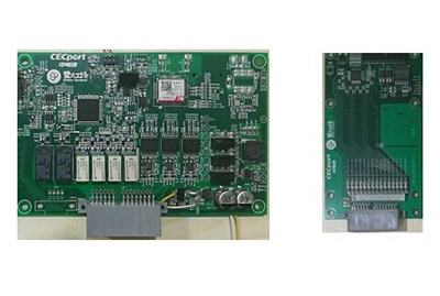
6. 烧录板:

7. 烧录时间参数:
Hex File Size : 43K
Erase time: 0.025s
Progarm time: 6.4s
Verify time: 5.7s
Total Progarm time: 12.2s
8. 产品特性:
1. 安全性高,烧录板主控MCU和被烧录MCU都设置读保护(ROP),文件升级读保护后无法读出.
2. 脱机烧写,1拖4的烧录,烧录采用各烧各的方式,烧写时无需电脑,方便生产线上使用.
3. 编程速度快, 已经做到整个烧录43K大小的文件只需12.2s.
4. 支持裸片烧写.
5. 芯片正确放入后自动上电.
总结:
STM32烧录器实现脱机烧录.安全性高.烧写速度快.采用1拖4的烧录方式.烧写操作便捷.自动上电等特点,满足生产线上大批量
的烧写需求,大大提高烧录效率. 节省生产成本.
STM32烧录器解决方案成功地解决了原厂提供MCU烧录中的不足,为推广高性价比STM32提供便利,使更多人受益于ST的产品.
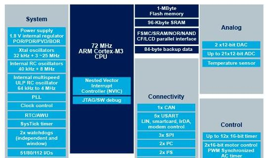
【STM32F103VG】
Mainstream Performance line, ARM Cortex-M3 MCU with 1 Mbyte Flash, 72 MHz CPU, motor control, USB and CAN
The STM32F103xF and STM32F103xG performance line family incorporates the high-performance ARM®Cortex®-M3 32-bit RISC core operating at a 72 MHz frequency, high-speed embedded memories (Flash memory up to 1 Mbyte and SRAM up to 96 Kbytes), and an extensive range of enhanced I/Os and peripherals connected to two APB buses. All devices offer three 12-bit ADCs, ten general-purpose 16-bit timers plus two PWM timers, as well as standard and advanced communication interfaces: up to two I2Cs, three SPIs, two I2Ss, one SDIO, five USARTs, an USB and a CAN.
The STM32F103xF/G XL-density performance line family operates in the –40 to +105 °C temperature range, from a 2.0 to 3.6 V power supply. A comprehensive set of power-saving mode allows the design of low-power applications.
These features make the STM32F103xF/G high-density performance line microcontroller family suitable for a wide range of applications such as motor drives, application control, medical and handheld equipment, PC and gaming peripherals, GPS platforms, industrial applications, PLCs, inverters, printers, scanners, alarm systems and video intercom.
主要特性
Core: ARM® 32-bit Cortex®-M3 CPU with MPU
72 MHz maximum frequency, 1.25 DMIPS/MHz (Dhrystone 2.1) performance at 0 wait state memory access
Single-cycle multiplication and hardware division
Memories
768 Kbytes to 1 Mbyte of Flash memory
96 Kbytes of SRAM
Flexible static memory controller with 4 Chip Select. Supports Compact Flash, SRAM, PSRAM, NOR and NAND memories
LCD parallel interface, 8080/6800 modes
Clock, reset and supply management
2.0 to 3.6 V application supply and I/Os
POR, PDR, and programmable voltage detector (PVD)
4-to-16 MHz crystal oscillator
Internal 8 MHz factory-trimmed RC
Internal 40 kHz RC with calibration
32 kHz oscillator for RTC with calibration
Low power
Sleep, Stop and Standby modes
VBATsupply for RTC and backup registers
3 × 12-bit, 1 μs A/D converters (up to 21 channels)
Conversion range: 0 to 3.6 V
Triple-sample and hold capability
Temperature sensor
2 × 12-bit D/A converters
DMA: 12-channel DMA controller
Supported peripherals: timers, ADCs, DAC, SDIO, I2Ss, SPIs, I2Cs and USARTs
Debug mode
Serial wire debug (SWD) & JTAG interfaces
Cortex®-M3 Embedded Trace Macrocell™
Up to 112 fast I/O ports
51/80/112 I/Os, all mappable on 16 external interrupt vectors and almost all 5 V-tolerant
Up to 17 timers
Up to ten 16-bit timers, each with up to 4 IC/OC/PWM or pulse counter and quadrature (incremental) encoder input
2 × 16-bit motor control PWM timers with dead-time generation and emergency stop
2 × watchdog timers (Independent and Window)
SysTick timer: a 24-bit downcounter
2 × 16-bit basic timers to drive the DAC
Up to 13 communication interfaces
Up to 2 × I2C interfaces (SMBus/PMBus)
Up to 5 USARTs (ISO 7816 interface, LIN, IrDA capability, modem control)
Up to 3 SPIs (18 Mbit/s), 2 with I2S interface multiplexed
CAN interface (2.0B Active)
USB 2.0 full speed interface
SDIO interface
CRC calculation unit, 96-bit unique ID
ECOPACK®packages
电路原理图
【STM32F103RE】
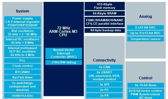
Mainstream Performance line, ARM Cortex-M3 MCU with 512 Kbytes Flash, 72 MHz CPU, motor control, USB and CAN
The STM32F103xC, STM32F103xD and STM32F103xE performance line family incorporates the high-performance ARM® Cortex®-M3 32-bit RISC core operating at a 72 MHz frequency, high-speed embedded memories (Flash memory up to 512 Kbytes and SRAM up to 64 Kbytes), and an extensive range of enhanced I/Os and peripherals connected to two APB buses. All devices offer three 12-bit ADCs, four general-purpose 16-bit timers plus two PWM timers, as well as standard and advanced communication interfaces: up to two I2Cs, three SPIs, two I2Ss, one SDIO, five USARTs, an USB and a CAN.
The STM32F103xC/D/E high-density performance line family operates in the –40 to +105 °C temperature range, from a 2.0 to 3.6 V power supply. A comprehensive set of power-saving mode allows the design of low-power applications.
These features make the STM32F103xC/D/E high-density performance line microcontroller family suitable for a wide range of applications such as motor drives, application control, medical and handheld equipment, PC and gaming peripherals, GPS platforms, industrial applications, PLCs, inverters, printers, scanners, alarm systems video intercom, and HVAC.
KEY FEATURES
Core: ARM® 32-bit Cortex®-M3 CPU
72 MHz maximum frequency, 1.25 DMIPS/MHz (Dhrystone 2.1) performance at 0 wait state memory access
Single-cycle multiplication and hardware division
Memories
256 to 512 Kbytes of Flash memory
up to 64 Kbytes of SRAM
Flexible static memory controller with 4 Chip Select. Supports Compact Flash, SRAM, PSRAM, NOR and NAND memories
LCD parallel interface, 8080/6800 modes
Clock, reset and supply management
2.0 to 3.6 V application supply and I/Os
POR, PDR, and programmable voltage detector (PVD)
4-to-16 MHz crystal oscillator
Internal 8 MHz factory-trimmed RC
Internal 40 kHz RC with calibration
32 kHz oscillator for RTC with calibration
Low power
Sleep, Stop and Standby modes
VBAT supply for RTC and backup registers
3 × 12-bit, 1 μs A/D converters (up to 21 channels)
Conversion range: 0 to 3.6 V
Triple-sample and hold capability
Temperature sensor
2 × 12-bit D/A converters
DMA: 12-channel DMA controller
Supported peripherals: timers, ADCs, DAC, SDIO, I2Ss, SPIs, I2Cs and USARTs
Debug mode
Serial wire debug (SWD) & JTAG interfaces
Cortex®-M3 Embedded Trace Macrocell™
Up to 112 fast I/O ports
51/80/112 I/Os, all mappable on 16 external interrupt vectors and almost all 5 V-tolerant
Up to 11 timers
Up to four 16-bit timers, each with up to 4 IC/OC/PWM or pulse counter and quadrature (incremental) encoder input
2 × 16-bit motor control PWM timers with dead-time generation and emergency stop
2 × watchdog timers (Independent and Window)
SysTick timer: a 24-bit downcounter
2 × 16-bit basic timers to drive the DAC
Up to 13 communication interfaces
Up to 2 × I2C interfaces (SMBus/PMBus)
Up to 5 USARTs (ISO 7816 interface, LIN, IrDA capability, modem control)
Up to 3 SPIs (18 Mbit/s), 2 with I2S interface multiplexed
CAN interface (2.0B Active)
USB 2.0 full speed interface
SDIO interface
CRC calculation unit, 96-bit unique ID
ECOPACK® packages
Circuit Diagram
责任编辑:David
【免责声明】
1、本文内容、数据、图表等来源于网络引用或其他公开资料,版权归属原作者、原发表出处。若版权所有方对本文的引用持有异议,请联系拍明芯城(marketing@iczoom.com),本方将及时处理。
2、本文的引用仅供读者交流学习使用,不涉及商业目的。
3、本文内容仅代表作者观点,拍明芯城不对内容的准确性、可靠性或完整性提供明示或暗示的保证。读者阅读本文后做出的决定或行为,是基于自主意愿和独立判断做出的,请读者明确相关结果。
4、如需转载本方拥有版权的文章,请联系拍明芯城(marketing@iczoom.com)注明“转载原因”。未经允许私自转载拍明芯城将保留追究其法律责任的权利。
拍明芯城拥有对此声明的最终解释权。


 产品分类
产品分类




 2012- 2022 拍明芯城ICZOOM.com 版权所有 客服热线:400-693-8369 (9:00-18:00)


