


 产品分类
产品分类
基于Digilentinc公司的Microchip PIC32MX3XX 32位MCU开发方案
 126
126
 拍明
拍明
原标题:Digilentinc Microchip PIC32MX3XX 32位MCU开发方案
microchip公司的PIC32MX系列产品采用5级流水线MIPS32® M4K® 32位内核,具有1.65 DMIPS/MHz性能,集成了512 KB闪存和128 KB 高速SRAM,100 MHz内部总线和缓存, 工作温度-40°C到105°C,工作电压2.3V-3.6V,主要用在高性能图像/用户接口,以太网/USB/CAN连接, 多任务嵌入控制和高性能音频等.本文介绍了PIC32MX3XX/4XX系列产品主要特性和框图, MIPS32® M4K®处理器内核主要特性和框图,以及chipKIT uC32开源开发平台主要特性,主要元件分布图和电路图.
PIC32MX3XX/4XX High-Performance,General Purpose and USB,32-bit Flash Microcontrollers
PIC32MX3XX/4XX系列产品主要特性:
High-Performance 32-bit RISC CPU:
• MIPS32® M4K® 32-bit core with 5-stage pipeline
• 80 MHz maximum frequency
• 1.56 DMIPS/MHz (Dhrystone 2.1) performance at 0 wait state Flash access
• Single-cycle multiply and high-performance divide unit
• MIPS16e® mode for up to 40% smaller code size
• Two sets of 32 core register files (32-bit) to reduce interrupt latency
• Prefetch Cache module to speed execution from Flash
Microcontroller Features:
• Operating temperature range of -40ºC to +105ºC
• Operating voltage range of 2.3V to 3.6V
• 32K to 512K Flash memory (plus an additional 12 KB of boot Flash)
• 8K to 32K SRAM memory
• Pin-compatible with most PIC24/dsPIC® DSC devices
• Multiple power management modes
• Multiple interrupt vectors with individually programmable priority
• Fail-Safe Clock Monitor Mode
• Configurable Watchdog Timer with on-chip
Low-Power RC Oscillator for reliable operation
Peripheral Features:
• Atomic SET, CLEAR and INVERT operation on select peripheral registers
• Up to 4-channel hardware DMA with automatic data size detection
• USB 2.0-compliant full-speed device and On-The-Go (OTG) controller
• USB has a dedicated DMA channel
• 3 MHz to 25 MHz crystal oscillator
• Internal 8 MHz and 32 kHz oscillators
• Separate PLLs for CPU and USB clocks
• Two I2C™ modules
• Two UART modules with:
- RS-232, RS-485 and LIN support
- IrDA® with on-chip hardware encoder and decoder
• Up to two SPI modules
• Parallel Master and Slave Port (PMP/PSP) with
8-bit and 16-bit data and up to 16 address lines
• Hardware Real-Time Clock and Calendar (RTCC)
• Five 16-bit Timers/Counters (two 16-bit pairs combine to create two 32-bit timers)
• Five capture inputs
• Five compare/PWM outputs
• Five external interrupt pins
• High-Speed I/O pins capable of toggling at up to 80 MHz
• High-current sink/source (18 mA/18 mA) on all I/O pins
• Configurable open-drain output on digital I/O pins
Debug Features:
• Two programming and debugging Interfaces:
- 2-wire interface with unintrusive access and real-time data exchange with application
- 4-wire MIPS® standard enhanced JTAG interface
• Unintrusive hardware-based instruction trace
• IEEE Standard 1149.2-compatible (JTAG) boundary scan
Analog Features:
• Up to 16-channel 10-bit Analog-to-Digital Converter:
- 1000 ksps conversion rate
- Conversion available during Sleep, Idle
• Two Analog Comparators
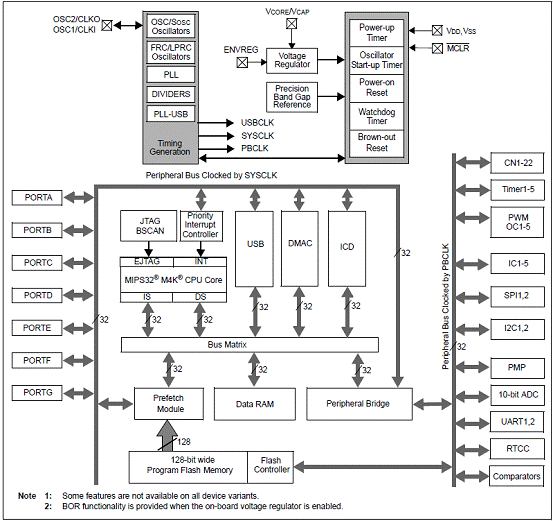
图1. PIC32MX3XX/4XX系列框图
MIPS32® M4K®处理器内核
The MIPS32® M4K® Processor Core is the heart of the PIC32MX3XX/4XX family processor. The CPU fetches instructions, decodes each instruction, fetches source operands, executes each instruction and writes the results of instruction execution to the proper destinations.
MIPS32® M4K®处理器内核主要特性:
• 5-stage pipeline
• 32-bit Address and Data Paths
• MIPS32 Enhanced Architecture (Release 2)
- Multiply-Accumulate and Multiply-Subtract Instructions
- Targeted Multiply Instruction
- Zero/One Detect Instructions
- WAIT Instruction
- Conditional Move Instructions (MOVN, MOVZ)
- Vectored interrupts
- Programmable exception vector base
- Atomic interrupt enable/disable
- GPR shadow registers to minimize latency for interrupt handlers
- Bit field manipulation instructions
• MIPS16e® Code Compression
- 16-bit encoding of 32-bit instructions to improve code density
- Special PC-relative instructions for efficient loading of addresses and constants
- SAVE & RESTORE macro instructions for setting up and tearing down stack frames within subroutines
- Improved support for handling 8 and 16-bit data types
• Simple Fixed Mapping Translation (FMT) mechanism
• Simple Dual Bus Interface
- Independent 32-bit address and data busses
- Transactions can be aborted to improve interrupt latency
• Autonomous Multiply/Divide Unit
- Maximum issue rate of one 32x16 multiply per clock
- Maximum issue rate of one 32x32 multiply every other clock
- Early-in iterative divide. Minimum 11 and maximum 34 clock latency (dividend (rs) sign extension-dependent)
• Power Control
- Minimum frequency: 0 MHz
- Low-Power mode (triggered by WAIT instruction)
- Extensive use of local gated clocks
• EJTAG Debug and Instruction Trace
- Support for single stepping
- Virtual instruction and data address/value
- breakpoints
- PC tracing with trace compression
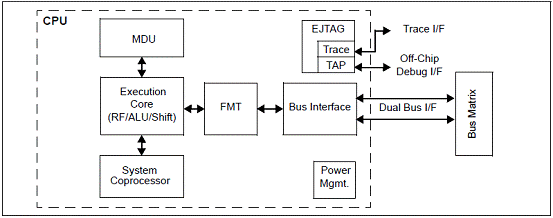
图2. MIPS32® M4K®处理器内核框图
chipKIT uC32开源开发平台
The chipKIT uC32 is based on the popular Arduino™ open-source hardware prototyping platform and adds the performance of the Microchip PIC32 microcontroller.
The uC32 is the same form factor as the Arduino™ Uno board and is compatible with many Arduino™ shields. It features a USB serial port interface for connection to the IDE and can be powered via USB or an external power supply.
The uC32 board takes advantage of the powerful PIC32MX340F512 microcontroller. This microcontroller features a 32-bit MIPS processor core running at 80Mhz, 512K of Flash program memory and 32K of SRAM data memory.
The uC32 can be programmed using the Multi-Platform Integrated Development Environment (MPIDE), an environment based on the original Arduino IDE modified to support PIC32. It contains everything needed to start developing embedded applications. In addition, the uC32 is fully compatible with the advanced Microchip MPLAB® IDE and the PICKit3 in-system programmer/debugger.
The uC32 is easy to use and suitable for both beginners and advanced users experimenting with electronics and embedded control systems.
The uC32 provides 42 I/O pins that support a number of peripheral functions, such as UART, SPI, and I2C ports and pulse width modulated outputs. Twelve of the I/O pins can be used as analog inputs or as digital inputs and outputs.
chipKIT uC32开源开发平台主要特性:
• Microchip® PIC32MX340F512H microcontroller (80 Mhz 32-bit MIPS, 512K Flash, 32K SRAM)
• compatible with many existing Arduino code samples and other resources
• Arduino Uno form factor
• compatible with many Arduino shields
• 42 available I/O pins
• two user LEDs
• PC connection uses a USB A > mini B cable (not included)
• 12 analog inputs
• 3.3V operating voltage
• 80Mhz operating frequency
• 75mA typical operating current
• 7V to 15V input voltage (recommended)
• 20V input voltage (maximum)
• 0V to 3.3V analog input voltage range
• +/-18mA DC current per pin
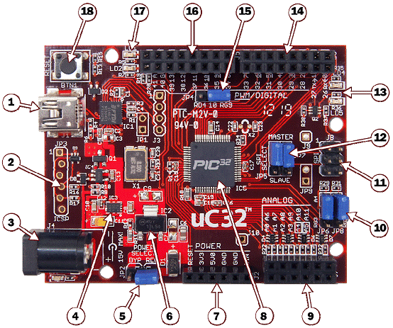
图3. chipKIT uC32开源开发平台外形图和元件分布图
chipKIT uC32开源开发平台主要元件说明:
1. USB Connector for USB Serial Converter
This connects to a USB port on the PC to provide the communications port for the MPIDE to talk to the uC32 board. This can also be used to power the uC32 board when connected to the PC.
2. JP3 – Microchip Debug Tool Connector
This connector is used to connect Microchip programmer/debugger tools, such as the PICkit™3. This allows the uC32 board to be used as a traditional microcontroller development board using the Microchip MPLAB® IDE.
3. J4 – External Power Connector
This is a 5.5mm x 2.1mm barrel connector used to power the uC32 board from an external power supply. It is wired with the center terminal as the positive supply voltage. The power supply voltage must be in the range 7V to 15V.
4. Power Supply – 3.3V Regulator
Voltage regulator for the 3.3V power supply. This power supply can provide up to 500mA of current.
5. JP2 – Power Select Jumper
This jumper is used to route power from the external power connector through the onboard 5V voltage regulator or to bypass the 5V regulator. The REG position routes power through the 5V regulator. The BYP position bypasses the on-board 5V regulator. With this jumper in the BYP position the maximum input voltage that can be applied at the external power connector is 6V.
6. Power Supply – 5V Regulator
This on-board 5V voltage regulator regulates the input voltage applied at the external power connector to 5V. This is used to power the 3.3V regulator and to provide 5V power to expansion shields. This regulator can provide up to 800mA of current.
7. J2 – Shield Power Connector
This connector provides power to I/O expansion shields connected to the board.
8. PIC32 Microcontroller
The PIC32MX340F512H microcontroller is the main processor for the board.
9. J7 – Analog Signal Connector
This connector provides access to analog/digital I/O pins on the microcontroller.
10. JP6/JP7 – A4/A5 Signal Select Jumpers
These jumpers are used to switch pins 9 and 11 on connector J7 between analog inputs A4 and A5 or the I2C signals SDA and SCL.
11. J8 – SPI Signal Connector
This connector provides alternative access to the SPI signals. This is used by some shields for access to the SPI bus.
12. JP5/JP7 – SPI Master/Slave Select Jumpers
These jumpers are used to switch the SPI signals for use of the uC32 board as an SPI master device or as an SPI slave device. Both jumpers should be switched together. Place the shorting blocks in the MASTER position for master operation and in the SLAVE position for slave operation. Normally, these jumpers are in the MASTER position.
13. User LEDs
Two LEDs connected to digital signal pins 13 and 43.
14. J6 – Digital Signal Connector
This connector provides access to digital I/O pins on the microcontroller.
15. JP4 – Pin 10 Signal Select Jumper
16. This jumper is used to switch connector J5 pin 5 (digital signal 10) between pulse width modulator (PWM) operation and SPI operation. The jumper is placed in the RD4 position for PWM output and in the RG9 position for SPI slave operation. The shorting block on this jumper will normally be in the RD4 position. The only time it normally needs to be in the RG9 is when using the Uno32 board as an SPI slave device.
17. J5 – Digital Signal Connector
This connector provides access to digital I/O pins on the microcontroller.
18. Communications Status LEDs
These LEDs indicate activity on the USB serial interface.
19. Reset Button
This button can be used to reset the microcontroller, restarting operation from the boot loader
责任编辑:HanFeng
【免责声明】
1、本文内容、数据、图表等来源于网络引用或其他公开资料,版权归属原作者、原发表出处。若版权所有方对本文的引用持有异议,请联系拍明芯城(marketing@iczoom.com),本方将及时处理。
2、本文的引用仅供读者交流学习使用,不涉及商业目的。
3、本文内容仅代表作者观点,拍明芯城不对内容的准确性、可靠性或完整性提供明示或暗示的保证。读者阅读本文后做出的决定或行为,是基于自主意愿和独立判断做出的,请读者明确相关结果。
4、如需转载本方拥有版权的文章,请联系拍明芯城(marketing@iczoom.com)注明“转载原因”。未经允许私自转载拍明芯城将保留追究其法律责任的权利。
拍明芯城拥有对此声明的最终解释权。
相关资讯
:
基于MC33771主控芯片的新能源锂电池管理系统解决方案

AMIC110 32位Sitara ARM MCU开发方案

基于AMIC110多协议可编程工业通信处理器的32位Sitara ARM MCU开发方案

基于展讯SC9820超低成本LTE芯片平台的儿童智能手表解决方案

基于TI公司的AM437x双照相机参考设计

基于MTK6580芯片的W2智能手表解决方案


 2012- 2022 拍明芯城ICZOOM.com 版权所有 客服热线:400-693-8369 (9:00-18:00)


