


 产品分类
产品分类
基于Atmel公司的ATmega256RFR2无线MCU解决方案
 125
125
 拍明
拍明
原标题:Atmel ATmega256RFR2无线MCU解决方案
Atmel公司的ATmega256/128/64RFR2是基于AVR增强RISC架构的8位低功耗MCU,集成了高数据速率(250kbps-2Mbps)的2.4GHz收发器和256KB闪存以及33个I/O引脚,无线收发器具有帧处理,杰出的接收灵敏度(-100dBm)和高发送功率(高达3.5dBm),非常适合无线通信.本文介绍了ATmega256/128 /64RFR2主要特性,框图与 AVR架构框图和ATmega256RFR2-EK 评估套件主要特性和框图,以及套件中的无线控制板RCB256RFR2, RCB遥控制板和传感器端板的主要特性,框图,电路图与材料清单,PCB元件布局图.
The ATmega256/128/64RFR2 is a low-power CMOS 8-bit microcontroller based on the AVR enhanced RISC architecture combined with a high data rate transceiver for the 2.4 GHz ISM band.By executing powerful instructions in a single clock cycle, the device achieves throughputs approaching 1 MIPS per MHz allowing the system designer to optimize power consumption versus processing speed.
The radio transceiver provides high data rates from 250 kb/s up to 2 Mb/s, frame handling, outstanding receiver sensitivity and high transmit output power enabling a very robust wireless communication.
ATmega256/128/64RFR2主要特性:
• Network support by hardware assisted Multiple PAN Address Filtering
• Advanced Hardware assisted Reduced Power Consumption
• High Performance, Low Power AVR® 8-Bit Microcontroller
• Advanced RISC Architecture
- 135 Powerful Instructions – Most Single Clock Cycle Execution
- 32x8 General Purpose Working Registers / On-Chip 2-cycle Multiplier
- Up to 16 MIPS Throughput at 16 MHz and 1.8V – Fully Static Operation
• Non-volatile Program and Data Memories
- 256K/128K/64K Bytes of In-System Self-Programmable Flash
• Endurance: 10’000 Write/Erase Cycles @ 125°C (25’000 Cycles @ 85°C)
- 8K/4K/2K Bytes EEPROM
• Endurance: 20’000 Write/Erase Cycles @ 125°C (100’000 Cycles @ 25°C)
- 32K/16K/8K Bytes Internal SRAM
• JTAG (IEEE std. 1149.1 compliant) Interface
- Boundary-scan Capabilities According to the JTAG Standard
- Extensive On-chip Debug Support
- Programming of Flash EEPROM, Fuses and Lock Bits through the JTAG interface
• Peripheral Features
- Multiple Timer/Counter & PWM channels
- Real Time Counter with Separate Oscillator
- 10-bit, 330 ks/s A/D Converter; Analog Comparator; On-chip Temperature Sensor
- Master/Slave SPI Serial Interface
- Two Programmable Serial USART
- Byte Oriented 2-wire Serial Interface
• Advanced Interrupt Handler and Power Save Modes
• Watchdog Timer with Separate On-Chip Oscillator
• Power-on Reset and Low Current Brown-Out Detector
• Fully integrated Low Power Transceiver for 2.4 GHz ISM Band
- High Power Amplifier support by TX spectrum side lobe suppression
- Supported Data Rates: 250 kb/s and 500 kb/s, 1 Mb/s, 2 Mb/s
- -100 dBm RX Sensitivity; TX Output Power up to 3.5 dBm
- Hardware Assisted MAC (Auto-Acknowledge, Auto-Retry)
- 32 Bit IEEE 802.15.4 Symbol Counter
- SFD-Detection, Spreading; De-Spreading; Framing ; CRC-16 Computation
- Antenna Diversity and TX/RX control / TX/RX 128 Byte Frame Buffer
- Phase measurement support
• PLL synthesizer with 5 MHz and 500 kHz channel spacing for 2.4 GHz ISM Band
• Hardware Security (AES, True Random Generator)
• Integrated Crystal Oscillators (32.768 kHz & 16 MHz, external crystal needed)
• I/O and Package
- 38 Programmable I/O Lines
- 64-pad QFN (RoHS/Fully Green)
• Temperature Range: -40°C to 125°C Industrial
• Ultra Low Power consumption (1.8 to 3.6V) for AVR & Rx/Tx: 10.1mA/18.6 mA
- CPU Active Mode (16MHz): 4.1 mA
- 2.4GHz Transceiver: RX_ON 6.0 mA / TX 14.5 mA (maximum TX output power)
- Deep Sleep Mode: <700nA @ 25°C
• Speed Grade: 0 – 16 MHz @ 1.8 – 3.6V range with integrated voltage regulators
ATmega256/128/64RFR2应用:
• ZigBee® / IEEE 802.15.4-2011/2006/2003™ – Full and Reduced Function Device
• General Purpose 2.4GHz ISM Band Transceiver with Microcontroller
• RF4CE, SP100, WirelessHART™, ISM Applications and IPv6 / 6LoWPAN

图1. ATmega256/128/64RFR2框图
The AVR core combines a rich instruction set with 32 general purpose workingregisters. All 32 registers are directly connected to the Arithmetic Logic Unit (ALU). Two independent registers can be accessed with one single instruction executed in one clock cycle. The resulting architecture is very code efficient while achieving throughputs up to ten times faster than conventional CISC microcontrollers. The system includes internal voltage regulation and an advanced power management. Distinguished by the small leakage current it allows an extended operation time from battery.
The radio transceiver is a fully integrated ZigBee solution using a minimum number of external components. It combines excellent RF performance with low cost, small size and low current consumption. The radio transceiver includes a crystal stabilized fractional-N synthesizer, transmitter and receiver, and full Direct Sequence Spread Spectrum Signal (DSSS) processing with spreading and despreading. The device is fully compatible with IEEE802.15.4-2011/2006/2003 and ZigBee standards.
The ATmega256/128/64RFR2 provides the following features: 256K/128K/64K Bytes of In-System Programmable (ISP) Flash with read-while-write capabilities, 8K/4K/2K Bytes EEPROM, 32K/16K/8K Bytes SRAM, up to 35 general purpose I/O lines, 32 general purpose working registers, Real Time Counter (RTC), 6 flexible Timer/Counters with compare modes and PWM, a 32 bit Timer/Counter, 2 USART, a byte oriented 2-wire Serial Interface, a 8 channel, 10 bit analog to digital converter (ADC) with an optional differential input stage with programmable gain, programmable Watchdog Timer with Internal Oscillator, a SPI serial port, IEEE std. 1149.1 compliant JTAG test interface, also used for accessing the On-chip Debug system and programming and 6 software selectable power saving modes.
The Idle mode stops the CPU while allowing the SRAM, Timer/Counters, SPI port, and interrupt system to continue functioning. The Power-down mode saves the register contents but freezes the Oscillator, disabling all other chip functions until the next interrupt or hardware reset. In Power-save mode, the asynchronous timer continues to run, allowing the user to maintain a timer base while the rest of the device is sleeping.
The ADC Noise Reduction mode stops the CPU and all I/O modules except asynchronous timer and ADC, to minimize switching noise during ADC conversions. In Standby mode, the RC oscillator is running while the rest of the device is sleeping. This allows very fast start-up combined with low power consumption. In Extended Standby mode, both the main RC oscillator and the asynchronous timer continue to run.
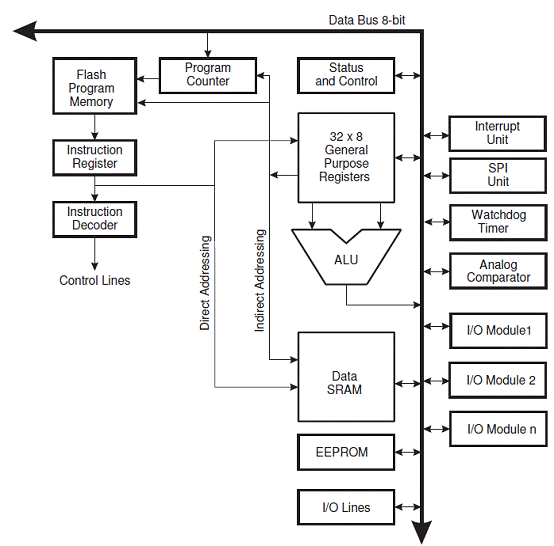
图2. ATmega256/128/64RFR2中AVR架构框图
ATmega256RFR2-EK 评估套件
The ATmega256RFR2 evaluation kit demonstrates the unique performance of the latest Atmel 2.4GHz System-on-chip solution, ATmega256RFR2. The kit is the hardware platform for evaluating complete wireless system solutions including wireless stacks such as IPv6/6LoWPAN, ZigBee RF4CE and ZigBee PRO. The kit is also an ideal platform evaluation and development of various proprietary sytems using low level drivers or the new Atmel Lightweight Mesh Stack.
The kit contains two radio controller boards (RCB) assembled with the ATmega256RFR2. The RCB is powered by two AAA batteries and forms a fully functional and portable wireless node. The kit also includes a sensor terminal board (STB) for connection to a PC/laptop, and one Key Remote Control Board enabling demo/evaluation of remote control applications like ZigBee Remote Control and ZigBee Light Link.
ATmega256RFR2-EK 评估板主要特性:
• Evaluation platform for the Atmel® ATmega256RFR2 using programmed performance test measurement application consisting of simple range measurement and packet error rate measurement
• Test various IEEE® 802.15.4 hardware embedded features
• Experiment with the enhanced feature set of ATmega256RFR2
• Use serial boot loader functionality to flash new application software image into the MCU’s program memory
• Enabled for demo/evaluation of remote control applications like ZigBee® Remote Control and ZigBee Light Link
• Extendable to any IEEE 802.15.4-based wireless application development such as ZigBee, 6LowPAN, ISA100, or any other proprietary network protocol

图3. ATmega256RFR2-EK 评估套件外形图
ATmega256RFR2-EK 评估套件硬件包括:
2 x RCB256RFR2 Radio Controller Board (RCB)
1 x RCB Sensor Terminal Board (STB)
1 x RCB Key Remote Control board (KEY_RC)
1 x RCB-BB RS232 cable
1 x USB cable
2 x 2.4GHz antenna
4 x AAA battery
The RCB256RFR2
The RCB256RFR2 is a small, battery-powered reference board that carries one Atmel ATmega256RFR2 System on Chip. It represents a system hardware reference for this microcontroller and contains a battery holder, SMA antenna connector and a 2x30 pin connector that allows the use of this board together with several different base boards to support various kinds of RF applications.
The RCB256RFR2 is designed to provide a reference design for the Atmel ATmega256RFR2 single-chip microcontroller and radio transceiver. The IC integrates a powerful, 8-bit AVR® RISC microcontroller, an IEEE 802.15.4™-compliant transceiver, and additional peripheral features. The built-in radio transceiver supports the worldwide accessible 2.4GHz ISM band.
The system is designed to demonstrate standard-based applications such as ZigBee/IEEE 802.15.4, ZigBee RF4CE, and 6LoWPAN, as well as high data rate ISM applications. The SMA antenna connector allows either operation with the antenna provided with the RCB or conducted RF performance measurements.
The RF section has been shielded to eliminate interference from sources external to the ATmega256RFR2. To investigate the reference design area, the shield can be opened by removing the snap-in cover while the RCB is not in operation.
Most peripheral features of the ATmega256RFR2 are made available through two expansion connectors (EXT0/1). There are a variety of base boards available for the RCB family.
RCB256RFR2主要特性
Stand-alone operable radio controller board (RCB)
• Design based on the single-chip Atmel® ATmega256RFR2 to support IEEE® 802.15.4, ZigBee®, 6LoWPAN, RF4CE, SP100, WirelessHART®, and ISM applications
• FCC-ID: VW4A091786
• SMA RF connector
• Simple user interface with button and LEDs
• Board information EEPROM containing
• MAC address
• Board identification, features, and serial number
• Crystal calibration values
• 2 × AAA batteries for stand-alone operation
• 60-pin extension connector to interface with application-specific hardware

图4.RCB256RFR2 PCBA外形图

图5.RCB256RFR2无线电控制板框图
RCB256RFR2无线电控制板材料清单:

The RCB Key Remote Control board (RCB遥控制板)
The RCB Key Remote Control board is a remote control type base board that offers a typical remote control user interface like buttons, but also contains elements of more advanced remote controls like a display and LEDs as event indicators.
It provides the standard 2x30 pin connector that is used on the Radio Controller Board platform and allows the connection of different types of RCBs to demonstrate different RF remote control applications and features.
This board has also external connectors for serial interface as well as a JTAG connector and can be used as development and programming base board for updating the firmware on the RCB’s microcontroller.
RCB遥控制板主要特性:
• Connector interface to adapt various radio controller boards (RCB)
• RCB battery powered, hand-held evaluation, and development platform
• 25 keys
• 5 LEDs
• 128 x 32 graphic display
• Analog, three-axis acceleration sensor
• 980nm IR transmitter
• RS232 and JTAG interfaces

图. RCB遥控制板外形图
RCB遥控制板材料清单:


The Sensor Terminal board(传感器端板)
The Sensor Terminal board is an interface board for the small form factor Radio Controller boards. It supports the 2x30 pin connector of the RCB platforms and provides several additional external interfaces like USB or GPIOs. It also provides a JTAG connector and therefore also allows the firmware update of RCB’s plugged into the 2x30 pin connector.
It is used as interface board for enabling a user controllable target application and for PC-based RF performance measurements with the RCB platforms.
传感器端板主要特性别:
Radio controller board (RCB) general purpose I/O (GPIO) interface
- Screw terminals for connecting external circuitry
- Onboard GPIO circuit protection and digitally controlled relays
• Atmel® AVR® JTAGICE mkII and AVRISP programming access for RCBs
• USB to virtual COM port support via fast parallel bus connection
• External power circuitry
• External 32Kbyte SRAM
• Temperature sensor
• Low power consumption in RCB battery mode

图. 传感器端板外形图
传感器端板材料清单:


责任编辑:HanFeng
【免责声明】
1、本文内容、数据、图表等来源于网络引用或其他公开资料,版权归属原作者、原发表出处。若版权所有方对本文的引用持有异议,请联系拍明芯城(marketing@iczoom.com),本方将及时处理。
2、本文的引用仅供读者交流学习使用,不涉及商业目的。
3、本文内容仅代表作者观点,拍明芯城不对内容的准确性、可靠性或完整性提供明示或暗示的保证。读者阅读本文后做出的决定或行为,是基于自主意愿和独立判断做出的,请读者明确相关结果。
4、如需转载本方拥有版权的文章,请联系拍明芯城(marketing@iczoom.com)注明“转载原因”。未经允许私自转载拍明芯城将保留追究其法律责任的权利。
拍明芯城拥有对此声明的最终解释权。
相关资讯
:
基于MC33771主控芯片的新能源锂电池管理系统解决方案

AMIC110 32位Sitara ARM MCU开发方案

基于AMIC110多协议可编程工业通信处理器的32位Sitara ARM MCU开发方案

基于展讯SC9820超低成本LTE芯片平台的儿童智能手表解决方案

基于TI公司的AM437x双照相机参考设计

基于MTK6580芯片的W2智能手表解决方案


 2012- 2022 拍明芯城ICZOOM.com 版权所有 客服热线:400-693-8369 (9:00-18:00)


