


 产品分类
产品分类
基于ADI公司的ADP5053 Xilinx FPGA电源解决方案
 115
115
 拍明
拍明
原标题:ADI ADP5053 Xilinx FPGA电源解决方案
ADI公司的ADP5053是四路高性能DC/DC降压转换器,并集成了监测电路,看门狗定时器和手动重置,输入电压4.5V-15.0V,全温度范围内的输出精度±1.5%,可调开关频率250kHz-1.4MHz,固定/可调输出,主要用在小型基站,FPGA和处理器电源,安全和监视,医疗电子.本文介绍了ADP5053主要特性,框图, 典型应用电路图以及多种Xilinx FPGA电源解决方案详细电路图和材料清单.
The ADP5053 combines four high performance buck regulators, a supervisory circuit, a watchdog timer, and a manual reset in a 48-lead LFCSP package that meets demanding performance and board space requirements. The device enables direct connection to high input voltages up to 15.0 V with no preregulators.
Channel 1 and Channel 2 integrate high-side power MOSFET and low-side MOSFET drivers. External NFETs can be used in low-side power devices to achieve an efficiency optimized solution and deliver a programmable output current of 1.2 A, 2.5 A, or 4 A. Combining Channel 1 and Channel 2 in a parallel configuration can provide a single output with up to 8 A of current.
Channel 3 and Channel 4 integrate both high-side and low-side MOSFETs to deliver an output current of 1.2 A.
The switching frequency of the ADP5053 can be programmed or synchronized to an external clock. The ADP5053 contains a precision enable pin on each channel for easy power-up sequencing or adjustable UVLO threshold.
The ADP5053 contains supervisory circuits that monitor the voltage level. The watchdog timer can generate a reset if the WDI pin is not toggled within a preset timeout period. Processor reset mode or system power on/off switch mode can be selected for manual reset functionality.
ADP5053主要特性:
Wide input voltage range: 4.5 V to 15.0 V
±1.5% output accuracy over full temperature range
250 kHz to 1.4 MHz adjustable switching frequency
Adjustable/fixed output options via factory fuse
Power regulation
Channel 1 and Channel 2: programmable 1.2 A/2.5 A/4 A sync buck regulators with low-side FET driver
Channel 3 and Channel 4: 1.2 A sync buck regulators
Single 8 A output (Channel 1 and Channel 2 operated in parallel)
Precision enable with 0.8 V accurate threshold
Active output discharge switch
FPWM or automatic PWM/PSM selection
Frequency synchronization input or output
Optional latch-off protection on OVP/OCP failure
Power-good flag on selected channels
UVLO, OCP, and TSD protection
Open-drain processor reset with external adjustable threshold monitoring
Watchdog refresh input
Manual reset input
ADP5053应用:
Small cell base stations
FPGA and processor applications
Security and surveillance
Medical applications
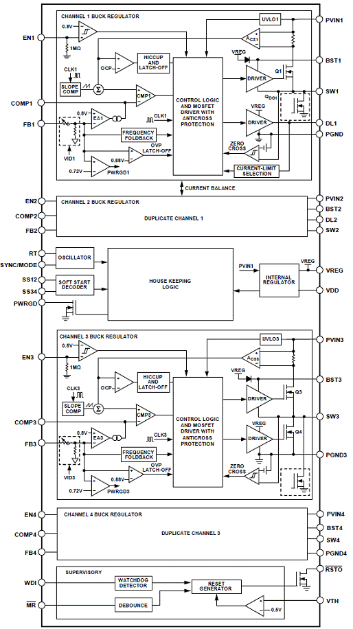
图1. ADP5053框图
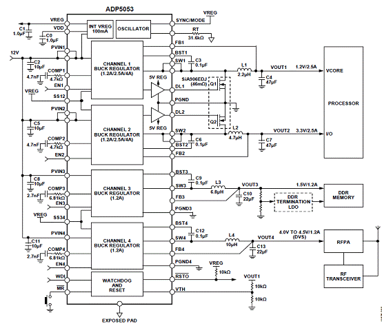
图2. ADP5053典型应用电路图:开关频率600kHz,固定输出模式
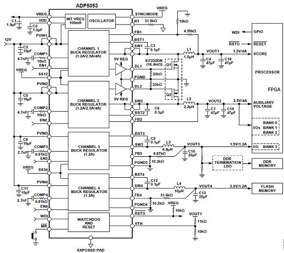
图3. ADP5053典型应用电路图:开关频率600kHz,可调输出模式

图4. ADP5053典型应用电路图:开关频率600kHz,可调输出模式,通路1/通路2并联输出

图5. ADP5053评估板外形图
Xilinx FPGA电源解决方案
Integrated Power Solutions for Xilinx FPGAs
Modern high performance FPGA-based systems require an increasing number of dedicated rails supplying core, I/O, memory, PLL, and precision analog voltages. Typical FPGA-based systems today make use of standalone switching regulators and LDOs; but, as board area continues to shrink as end product form factors shrink, this complicates the task of designing more efficient power management solutions for powering FPGAs. Combining multiple switching regulators and LDOs into a single package enables very small, flexible, highly efficient power management solutions for powering FPGAs and precision analog components with the highest system reliability.

图6. ADP5053 Xilinx FPGA电源框图
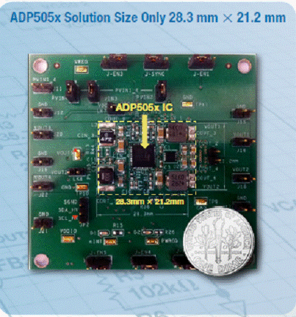
图7. ADP505x Xilinx FPGA电源解决方案外形图

图8. ADP5050 Xilinx FPGA Spartan-6电源解决方案电路框图
ADP5050 Xilinx FPGA Spartan-6电源解决方案材料清单:
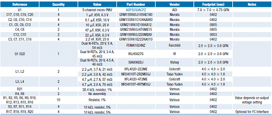
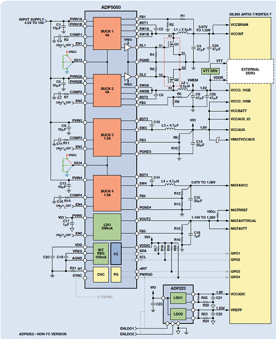
图9. ADP5050 Xilinx FPGA Artix-7/Kintex-7电源解决方案电路框图
ADP5050 Xilinx FPGA Artix-7/Kintex-7电源解决方案材料清单:
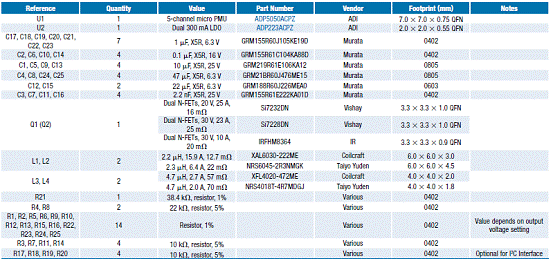
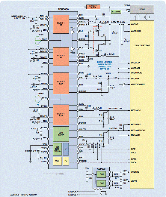
图10. ADP5050 Xilinx FPGA Virtex-7电源解决方案电路框图
ADP5050 Xilinx FPGA Virtex-7电源解决方案材料清单:

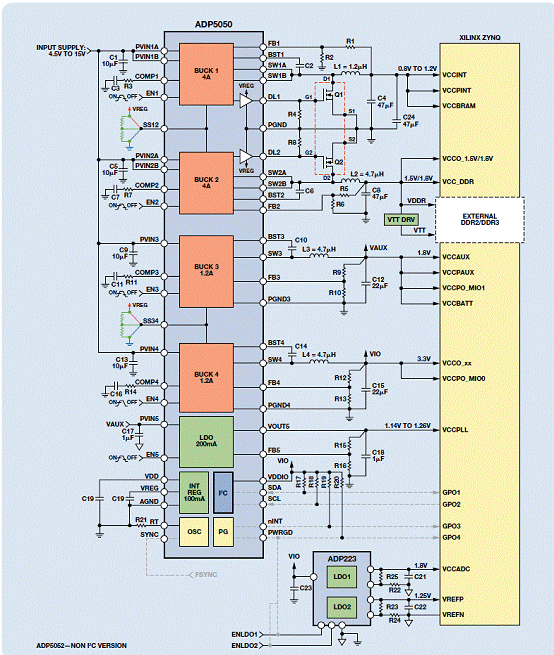
图11. ADP5050 Xilinx FPGA Zynq电源解决方案电路框图
ADP5050 Xilinx FPGA Zynq电源解决方案材料清单:

责任编辑:HanFeng
【免责声明】
1、本文内容、数据、图表等来源于网络引用或其他公开资料,版权归属原作者、原发表出处。若版权所有方对本文的引用持有异议,请联系拍明芯城(marketing@iczoom.com),本方将及时处理。
2、本文的引用仅供读者交流学习使用,不涉及商业目的。
3、本文内容仅代表作者观点,拍明芯城不对内容的准确性、可靠性或完整性提供明示或暗示的保证。读者阅读本文后做出的决定或行为,是基于自主意愿和独立判断做出的,请读者明确相关结果。
4、如需转载本方拥有版权的文章,请联系拍明芯城(marketing@iczoom.com)注明“转载原因”。未经允许私自转载拍明芯城将保留追究其法律责任的权利。
拍明芯城拥有对此声明的最终解释权。
相关资讯
:
基于MC33771主控芯片的新能源锂电池管理系统解决方案

AMIC110 32位Sitara ARM MCU开发方案

基于AMIC110多协议可编程工业通信处理器的32位Sitara ARM MCU开发方案

基于展讯SC9820超低成本LTE芯片平台的儿童智能手表解决方案

基于TI公司的AM437x双照相机参考设计

基于MTK6580芯片的W2智能手表解决方案


 2012- 2022 拍明芯城ICZOOM.com 版权所有 客服热线:400-693-8369 (9:00-18:00)


