


 产品分类
产品分类
基于On Semi公司的NCV8876汽车起-停控制解决方案
 156
156
 拍明
拍明
原标题:On Semi NCV8876汽车起-停控制解决方案
On Semi公司的NCV8876是汽车级起-停非同步升压控制器,能驱动外接N沟MOSFET.器件采用峰值电流模式控制和内部斜率补偿,保护特性包括逐个周期限流,保护和关断.主要用在汽车起动/停止控制.本文介绍了NCV8876主要特性和典型应用电路以及评估板NCV887601主要特性,电路图,材料厂清单和PCB布局图.
The NCV8876 is a Non-Synchronous Boost controller designed to supply a minimum output voltage during Start-Stop vehicle operation battery voltage sags. The controller drives an external N-channel MOSFET. The device uses peak current mode control with internal slope compensation. The IC incorporates an internal regulator that supplies charge to the gate driver.Protection features include, cycle-by-cycle current limiting, protection and thermal shutdown.
Additional features include low quiescent current sleep mode operation. The NCV8876 is enabled when the supply voltage drops below 7.3 V, with boost operation initiated when the supply voltage is below 6.8 V.
NCV8876主要特性:
• Automatic Enable Below 7.3 V (Factory Programmable)
• Boost Mode Operation at 6.8 V
• _2% Output Accuracy Over Temperature Range
• Peak Current Mode Control with Internal Slope Compensation
• Externally Adjustable frequency Operation
• Wide Input Voltage Range of 2 V to 40 V, 45 V Load Dump
• Low Quiescent Current in Sleep Mode (<11uA Typical)
• Cycle−by−Cycle Current Limit Protection
• Hiccup−Mode Overcurrent Protection (OCP)
• Thermal Shutdown (TSD)
• This is a Pb−Free Device
NCV8876典型应用:
• Applications Requiring Regulated Voltage through Cranking and Start−Stop Operation
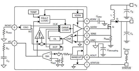
图1. NCV8876典型应用电路
评估板NCV887601
This NCV887601 evaluation board provides a convenient way to evaluate a high frequency boost controller designed to supply a minimum output voltage during Start-Stop vehicle battery voltage sags. The unit is in low Iq sleep-mode under normal battery operating condition and will wake-up when the monitored voltage drops below 7.3 V and begin regulating once 6.8 V is reached. Switching frequency is set to 440 kHz with a user selectable ROSC resistor. The evaluation board is rated 6.8 V / 3.6 A at a 2.6 V input voltage. Operation below 2.6 V is possible if output current is reduced.
评估板NCV887601主要特性:
• Automatic enable below 7.3 V
• Boost Operation at 6.8 V
• 440 kHz Switching Frequency
• Input Undervoltage Lockout
• Wide Input Voltage of 2.6 V to 45 V
• Low Quiescent Current in Sleep Mode (<11 uA Typical)
• Cycle-by-Cycle Current Limit Protection
• Status Monitoring
• Automotive Grade
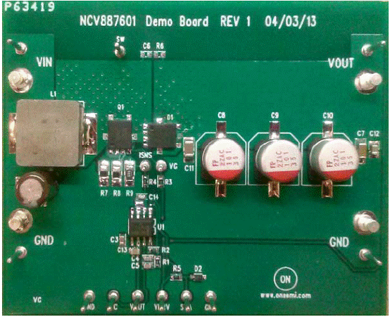
图2. 评估板NCV887601外形图
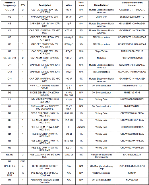
评估板NCV887601材料清单:
责任编辑:HanFeng
【免责声明】
1、本文内容、数据、图表等来源于网络引用或其他公开资料,版权归属原作者、原发表出处。若版权所有方对本文的引用持有异议,请联系拍明芯城(marketing@iczoom.com),本方将及时处理。
2、本文的引用仅供读者交流学习使用,不涉及商业目的。
3、本文内容仅代表作者观点,拍明芯城不对内容的准确性、可靠性或完整性提供明示或暗示的保证。读者阅读本文后做出的决定或行为,是基于自主意愿和独立判断做出的,请读者明确相关结果。
4、如需转载本方拥有版权的文章,请联系拍明芯城(marketing@iczoom.com)注明“转载原因”。未经允许私自转载拍明芯城将保留追究其法律责任的权利。
拍明芯城拥有对此声明的最终解释权。
相关资讯
:
基于MC33771主控芯片的新能源锂电池管理系统解决方案

AMIC110 32位Sitara ARM MCU开发方案

基于AMIC110多协议可编程工业通信处理器的32位Sitara ARM MCU开发方案

基于展讯SC9820超低成本LTE芯片平台的儿童智能手表解决方案

基于TI公司的AM437x双照相机参考设计

基于MTK6580芯片的W2智能手表解决方案


 2012- 2022 拍明芯城ICZOOM.com 版权所有 客服热线:400-693-8369 (9:00-18:00)


