


 产品分类
产品分类
基于ADI公司的ADuCM360 14位4-20mA热电偶温度测量系统解决方案
 93
93
 拍明
拍明
原标题:ADI ADuCM360 14位4-20mA热电偶温度测量系统解决方案
ADI公司的ADuCM360是全集成的3.9 kSPS, 24位数据采集系统,包括有两个高性能多路Sigma-Delta (Σ-Δ) ADC,一个32位ARM Cortex™-M3处理器和闪存/EE存储器,可编程ADC输出速率(3.5 Hz - 3.906 kHz),50/60Hz噪音抑制,RMS噪音,3.53Hz时为52nV,50Hz为200nV,主要用在工业自动化和过程控制,智能精密传感系统,4mA-20mA智能传感器系统,医疗设备和病人监护.本文介绍了ADuCM360主要特性,功能框图,典型系统配置图,以及采用ARM Cortex-M3的14位4-20mA回路供电的热电偶温度测量系统的优势和特性,电路图和PCB元件图.
The ADuCM360 is a fully integrated, 3.9 kSPS, 24-bit data acquisition system that incorporates dual high performance, multichannel sigma-delta (Σ-Δ) analog-to-digital converters (ADCs), a 32-bit ARM Cortex™-M3 processor, and Flash/EE memory on a single chip. The ADuCM360 is designed for direct interfacing to external precision sensors in both wired and battery-powered applications. The ADuCM361 contains all the features of the ADuCM360 except that only one 24-bit Σ-Δ ADC (ADC1) is available.
The ADuCM360/ADuCM361 contain an on-chip 32 kHz oscillator and an internal 16 MHz high frequency oscillator. The high frequency oscillator is routed through a programmable clock divider from which the operating frequency of the processor core clock is generated. The maximum core clock speed is 16 MHz; this speed is not limited by operating voltage or temperature.
The microcontroller core is a low power ARM Cortex-M3 processor, a 32-bit RISC machine that offers up to 20 MIPS peak performance. The Cortex-M3 processor incorporates a flexible, 11-channel DMA controller that supports all wired communica-tion peripherals (SPI, UART, and I2C). Also integrated on chip are 128 kB of nonvolatile Flash/EE memory and 8 kB of SRAM.
The analog subsystem consists of dual ADCs, each connected to a flexible input mux. Both ADCs can operate in fully differential and single-ended modes. Other on-chip ADC features include dual programmable excitation current sources, diagnostic current sources, and a bias voltage generator of AVDD_REG/2 (900 mV) to set the common-mode voltage of an input channel. A low-side internal ground switch is provided to allow power-down of an external circuit (for example, a bridge circuit) between conversions.
The ADCs contain two parallel filters: a sinc3 or sinc4 filter in parallel with a sinc2 filter. The sinc3 or sinc4 filter is used for precision measurements. The sinc2 filter is used for fast measure-ments and for the detection of step changes in the input signal.
The devices contain a low noise, low drift internal band gap ref-erence, but they can be configured to accept one or two external reference sources in ratiometric measurement configurations. An option to buffer the external reference inputs is provided on chip. A single-channel buffered voltage output DAC is also provided on chip.
The ADuCM360/ADuCM361 integrate a range of on-chip peripherals, which can be configured under microcontroller software control as required in the application. The peripherals include UART, I2C, and dual SPI serial I/O communication controllers; a 19-pin GPIO port; two general-purpose timers; a wake-up timer; and a system watchdog timer. A 16-bit PWM controller with six output channels is also provided.
The ADuCM360/ADuCM361 are specifically designed to operate in battery-powered applications where low power operation is critical. The microcontroller core can be configured in a normal operating mode that consumes 290 μA/MHz (including flash/ SRAM IDD). An overall system current consumption of 1 mA can be achieved with both ADCs on (input buffers off), PGA gain of 4, one SPI port on, and all timers on.
The ADuCM360/ADuCM361 can be configured in a number of low power operating modes under direct program control, including a hibernate mode (internal wake-up timer active) that consumes only 4 μA. In hibernate mode, peripherals such as external interrupts or the internal wake-up timer can wake up the device. This mode allows the part to operate with ultralow power and still respond to asynchronous external or periodic events.
On-chip factory firmware supports in-circuit serial download via a serial wire interface (2-pin JTAG system) and UART; non-intrusive emulation is also supported via the serial wire interface. These features are incorporated into a low cost QuickStart™ Development System that supports this precision analog micro-controller family.
The parts operate from an external 1.8 V to 3.6 V voltage supply and are specified over an industrial temperature range of −40℃ to +125℃.
ADuCM360主要特性:
Analog input/output
Dual 24-bit ADCs (ADuCM360)
Single 24-bit ADC (ADuCM361)
Programmable ADC output rate (3.5 Hz to 3.906 kHz)
Simultaneous 50 Hz/60 Hz noise rejection
At 50 SPS continuous conversion mode
At 16.67 SPS single conversion mode
Flexible input mux for input channel selection to both ADCs
Two 24-bit multichannel ADCs (ADC0 and ADC1)
6 differential or 11 single-ended input channels
4 internal channels for monitoring DAC, temperature sensor, IOVDD/4, and AVDD/4 (ADC1 only)
Programmable gain (1 to 128)
RMS noise: 52 nV at 3.53 Hz, 200 nV at 50 Hz
Programmable sensor excitation current sources
On-chip precision voltage reference
Single 12-bit voltage output DAC
NPN mode for 4 mA to 20 mA loop applications
Microcontroller
ARM Cortex-M3 32-bit processor
Serial wire download and debug
Internal watch crystal for wake-up timer
16 MHz oscillator with 8-way programmable divider
Memory
128 kB Flash/EE memory, 8 kB SRAM
In-circuit debug/download via serial wire and UART
Power supply range: 1.8 V to 3.6 V (maximum)
Power consumption, MCU active mode
Core consumes 290 μA/MHz
Overall system current consumption of 1.0 mA with core operating at 500 kHz (both ADCs on, input buffers off, PGA gain of 4, one SPI port on, and all timers on)
Power consumption, power-down mode: 4 μA (wake-up timer active)
On-chip peripherals
UART, I2C, and 2 × SPI serial I/O
16-bit PWM controller
19-pin multifunction GPIO port
2 general-purpose timers
Wake-up timer/watchdog timer
Multichannel DMA and interrupt controller
Package and temperature range
48-lead, 7 mm × 7 mm LFCSP
Specified for −40℃ to +125℃ operation
Development tools
Low cost QuickStart Development System
Third-party compiler and emulator tool support
Multiple functional safety features for improved diagnostics
ADuCM360应用:
Industrial automation and process control
Intelligent precision sensing systems
4 mA to 20 mA loop-powered smart sensor systems
Medical devices, patient monitoring
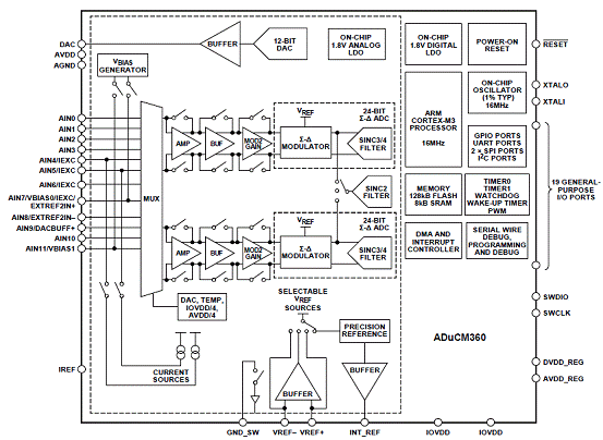
图1. ADuCM360功能框图
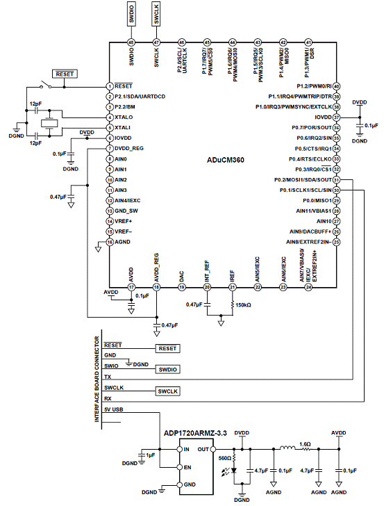
图2. ADuCM360典型系统配置图
采用ARM Cortex-M3的14位4-20mA回路供电的热电偶温度测量系统
热电偶温度测量系统优势和特性:
4-20mA thermocouple temperature monitor
Cold junction compensation
Loop powered
热电偶温度测量系统应用:
Field Instruments/ Smart Transmitters
Temperature Controllers
The circuit shown in Figure 3 is a complete loop powered thermocouple temperature measurement system where the 4 mA-to-20 mA output current is controlled using the PWM function of a precision analog microcontroller.
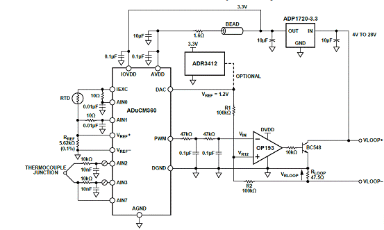
图3. ADuCM360控制的4-20mA的温度监视器电路图
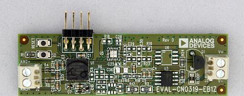
图4. 4-20mA的温度监视器外形图
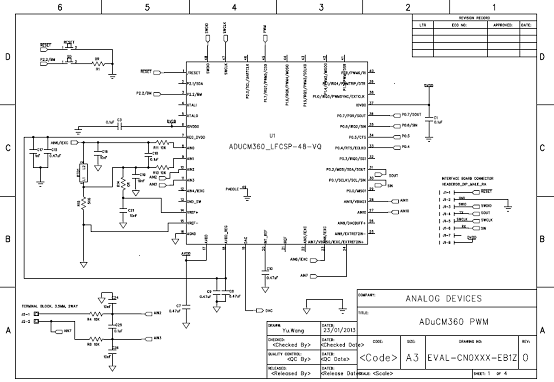
图5. 4-20mA的温度监视器电路图(1)
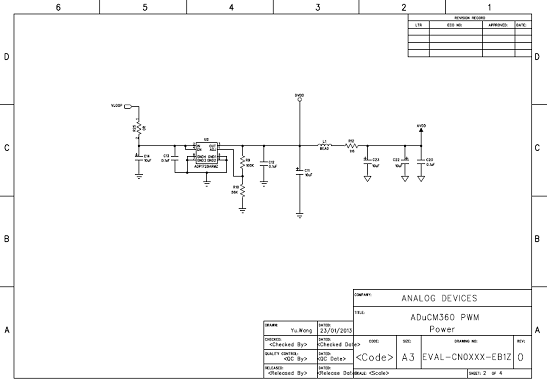
图6. 4-20mA的温度监视器电路图(2)
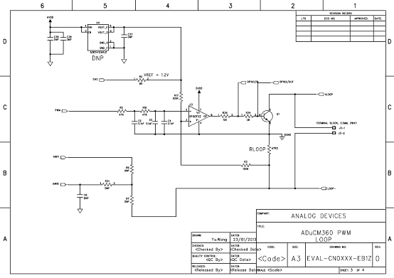
图7. 4-20mA的温度监视器电路图(3)
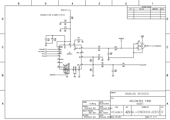
图8. 4-20mA的温度监视器电路图(4)
责任编辑:HanFeng
【免责声明】
1、本文内容、数据、图表等来源于网络引用或其他公开资料,版权归属原作者、原发表出处。若版权所有方对本文的引用持有异议,请联系拍明芯城(marketing@iczoom.com),本方将及时处理。
2、本文的引用仅供读者交流学习使用,不涉及商业目的。
3、本文内容仅代表作者观点,拍明芯城不对内容的准确性、可靠性或完整性提供明示或暗示的保证。读者阅读本文后做出的决定或行为,是基于自主意愿和独立判断做出的,请读者明确相关结果。
4、如需转载本方拥有版权的文章,请联系拍明芯城(marketing@iczoom.com)注明“转载原因”。未经允许私自转载拍明芯城将保留追究其法律责任的权利。
拍明芯城拥有对此声明的最终解释权。
相关资讯
:
基于MC33771主控芯片的新能源锂电池管理系统解决方案

AMIC110 32位Sitara ARM MCU开发方案

基于AMIC110多协议可编程工业通信处理器的32位Sitara ARM MCU开发方案

基于展讯SC9820超低成本LTE芯片平台的儿童智能手表解决方案

基于TI公司的AM437x双照相机参考设计

基于MTK6580芯片的W2智能手表解决方案


 2012- 2022 拍明芯城ICZOOM.com 版权所有 客服热线:400-693-8369 (9:00-18:00)


