基于ADI公司的AD7403高性能二阶Σ-Δ调制解决方案
 129
129
 拍明
拍明
原标题:ADI AD7403高性能二阶Σ-Δ调制解决方案
ADI公司的AD7403是高性能二阶Delta-Sigma调制器,能把模拟输入信号转换成高速单比特数据流,外时钟频率5-20MHz,16位不丢失码,SNR 88dB,温度漂移1.6 μV/℃, 满刻度输入范围±320 mV,工作温度−40℃ 到 + 125℃,主要用在马达控制,电源和太阳能逆变器,数据采集系统,风能逆变器,并联电流监视器等.本文介绍了AD7403主要特性,框图, 评估板EVAL-AD7403FMCZ主要特性,框图,电路图,材料清单和PCB元件布局图.
The AD7403 is a high performance, second-order, Σ-Δ modulator that converts an analog input signal into a high speed, single-bit data stream, with on-chip digital isolation based on Analog Devices, Inc., iCoupler® technology. The AD7403 operates from a 5 V (VDD1) power supply and accepts a differential input signal of ±250 mV (±320 mV full-scale). The differential input is ideally suited to shunt voltage monitoring in high voltage applications where galvanic isolation is required.
The analog input is continuously sampled by a high performance analog modulator, and converted to a ones density digital output stream with a data rate of up to 20 MHz. The original information can be reconstructed with an appropriate digital filter to achieve 88 dB signal to noise ratio (SNR) at 78.1 kSPS. The serial input/output can use a 5 V or a 3 V supply (VDD2).
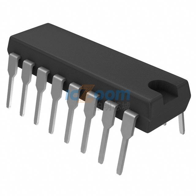
The serial interface is digitally isolated. High speed complementary metal oxide semiconductor (CMOS) technology, combined with monolithic transformer technology, means the on-chip isolation provides outstanding performance characteristics, superior to alternatives such as optocoupler devices. The AD7403 device is offered in a 16-lead, wide-body SOIC package and has an operating temperature range of −40℃ to +125℃.
AD7403主要特性:
5 MHz to 20 MHz external clock input rate
16 bits, no missing codes
Signal-to-noise ratio (SNR): 88 dB typical
Effective number of bits (ENOB): 14.2 bits typical
Typical offset drift vs. temperature: 1.6 μV/℃ typical
On-board digital isolator
On-board reference
Full-scale analog input range: ±320 mV
−40℃ to + 125℃ operating range
High common-mode transient immunity: >25 kV/μs
16-lead, wide-body SOIC, with increased creepage package
Slew rate limited output for low electromagnetic interference (EMI)
Safety and regulatory approvals (pending)
UL recognition
5000 V rms for 1 minute per UL 1577
CSA Component Acceptance Notice 5A
VDE Certificate of Conformity
DIN V VDE V 0884-10 (VDE V 0884-10):2006-12
VIORM = 1250 VPEAK
AD7403应用:
Shunt current monitoring
AC motor controls
Power and solar inverters
Wind turbine inverters
Data acquisition systems
Analog-to-digital and opto-isolator replacements

图1. AD7403框图
评估板EVAL-AD7403FMCZ
The EVAL-AD7403FMCZ is a full featured evaluation board designed to allow the user to easily evaluate all features of the AD7403 isolated analog-to-digital converter (ADC). The evaluation board can be controlled by the EVAL-SDP-CH1Z via FMCZ connector (J9). The SDP-H1 board (EVAL-SDP-CH1Z) allows the evaluation board to be controlled through a USB port of a PC using the evaluation board software available for download from the product page or from the included installer CD.
On-board components include the following:
ADuM6000: isolated iCoupler® 5kV, DC / DC converter
ADP2441: 36 V, 1A, synchronous, step down DC-DC regulator
ADP7104ARDZ-5.0: 5 V low noise LDO
评估板EVAL-AD7403FMCZ主要特性:
Full featured evaluation board for the AD7403
On-board power supplies
Standalone capability
System demonstration platform (SDP-H1) compatible (EVAL-SDP-CH1Z)
PC software for control and data analysis (CD with software included in evaluation kit)
评估板EVAL-AD7403FMCZ包括:
Evaluation board
CD containing evaluation board software installation
Additional Equipment Required
EVAL-SDP-CH1Z (must be ordered separately) includes a USB cable and 12v wall wart.
Signal source
PC running Windows XP SP3, Windows Vista, or Windows 7 with USB 2.0 port

图2.评估板EVAL-AD7403FMCZ(左)和EVAL-SDP-CH1Z(右)的建立图

图3.评估板EVAL-AD7403FMCZ框图

图4.评估板EVAL-AD7403FMCZ电路图(1)

图5.评估板EVAL-AD7403FMCZ电路图(2)
责任编辑:HanFeng
【免责声明】
1、本文内容、数据、图表等来源于网络引用或其他公开资料,版权归属原作者、原发表出处。若版权所有方对本文的引用持有异议,请联系拍明芯城(marketing@iczoom.com),本方将及时处理。
2、本文的引用仅供读者交流学习使用,不涉及商业目的。
3、本文内容仅代表作者观点,拍明芯城不对内容的准确性、可靠性或完整性提供明示或暗示的保证。读者阅读本文后做出的决定或行为,是基于自主意愿和独立判断做出的,请读者明确相关结果。
4、如需转载本方拥有版权的文章,请联系拍明芯城(marketing@iczoom.com)注明“转载原因”。未经允许私自转载拍明芯城将保留追究其法律责任的权利。
拍明芯城拥有对此声明的最终解释权。


 产品分类
产品分类



 2012- 2022 拍明芯城ICZOOM.com 版权所有 客服热线:400-693-8369 (9:00-18:00)


