基于TI公司的TMS320C6678高性能定-浮点DSP开发方案
 185
185
 拍明
拍明
原标题:TI TMS320C6678高性能定-浮点DSP开发方案
TI公司的TMS320C6678是采用TI KeyStone多核架构的高性能定/浮点数字信号处理器(DSP),内核处理速度高达1GHz,提供八个SMS320C66x™ DSP Core 子系统,1GHz定点性能为44.8 GMAC/核,1GHz浮点性能为22.4 GFLOP/核,具有多核共享存储器控制器(MSMC), 多核导航器和网络协处理器以及大量的外设,主要用在关键任务系统,高性能计算系统,通信和网络,音频和视频基础设备,图像和分析,媒体处理, 工业自动化以及自动化和过程控制.本文介绍了TMS320C6678主要特性,功能框图,以及评估板TMDSEVM6670L主要特性,电路图,材料清单和PCB元件布局图.
The SM320C6678 DSP is a highest-performance fixed/floating-point DSP that is based on TI’s KeyStone multicore architecture. Incorporating the new and innovative C66x DSP core, this device can run at a core speed of up to 1 GHz. For developers of a broad range of applications, such as mission critical, medical imaging, test and automation, and other applications requiring high performance, TI’s SM320C6678 DSP offers 8 GHz cumulative DSP and enables a platform that is power-efficient and easy to use. In addition, it is fully backward compatible with all existing C6000 family fixed and floating point DSPs.
TI’s KeyStone architecture provides a programmable platform integrating various subsystems (C66x cores, memory subsystem, peripherals, and accelerators) and uses several innovative components and techniques to maximize intra-device and inter-device communication that allows the various DSP resources to operate efficiently and seamlessly. Central to this architecture are key components such as Multicore Navigator that allows for efficient data management between the various device components. The TeraNet is a non-blocking switch fabric enabling fast and contention-free internal data movement. The multicore shared memory controller allows access to shared and external memory directly without drawing from switch fabric capacity.
For fixed-point use, the C66x core has 4× the multiply accumulate (MAC) capability of C64x+ cores. In addition, the C66x core integrates floating point capability and the per core raw computational performance is an industry-leading 32 GMACS/core and 16 GFLOPS/core (@1 GHz operating frequency). It can execute 8 single precision floating point MAC operations per cycle and can perform double- and mixed-precision operations and is IEEE754 compliant. The C66x core incorporates 90 new instructions (compared to the C64x+ core) targeted for floating point and vector math oriented processing. These enhancements yield sizeable performance improvements in popular DSP kernels used in signal processing, mathematical, and image acquisition functions. The C66x core is backwards code compatible with TI’s previous generation C6000 fixed and floating point DSP cores, ensuring software portability and shortened software development cycles for applications migrating to faster hardware.
The C6678 DSP integrates a large amount of on-chip memory. In addition to 32KB of L1 program and data cache, there is 512KB of dedicated memory per core that can be configured as mapped RAM or cache. The device also integrates 4096KB of Multicore Shared Memory that can be used as a shared L2 SRAM and/or shared L3 SRAM. All L2 memories incorporate error detection and error correction. For fast access to external memory, this device includes a 64-bit DDR-3 external memory interface (EMIF) running at 1600 MHz and has ECC DRAM support.
This family supports a plethora of high speed standard interfaces including RapidIO ver 2, PCI Express Gen2, and Gigabit Ethernet, as well as an integrated Ethernet switch. It also includes I2C, UART, Telecom Serial Interface Port (TSIP), and a 16-bit EMIF, along with general purpose CMOS IO. For high throughput, low latency communication between devices or with an FPGA, this device also sports a 25-Gbaud full-duplex interface called HyperLink. Adding to the network awareness of this device is a network co-processor that includes both packet and optional security acceleration. The packet accelerator can process up to 1.5 M packets/s and enables a single IP address to be used for the entire multicore C6678 device. It also provides L2 to L4 classification, along with checksum and QoS capabilities.
The C6678 device has a complete set of development tools, which includes: an enhanced C compiler, an assembly optimizer to simplify programming and scheduling, and a WindowsR debugger interface for visibility into source code execution.
TMS320C6678主要特性:
• Eight SMS320C66x™ DSP Core Subsystems (C66x CorePacs), Each with
– 1.0 GHz C66x Fixed/Floating-Point CPU Core
› 44.8 GMAC/Core for Fixed Point @ 1 GHz
› 22.4 GFLOP/Core for Floating Point @ 1 GHz
– Memory
› 32K Byte L1P Per Core
› 32K Byte L1D Per Core
› 512K Byte Local L2 Per Core
• Multicore Shared Memory Controller (MSMC)
– 4096KB MSM SRAM Memory Shared by Eight DSP C66x CorePacs
– Memory Protection Unit for Both MSM SRAM and DDR3_EMIF
• Multicore Navigator
– 8192 Multipurpose Hardware Queues with Queue Manager
– Packet-Based DMA for Zero-Overhead Transfers
• Network Coprocessor
– Packet Accelerator Enables Support for
› Transport Plane IPsec, GTP-U, SCTP, PDCP
› L2 User Plane PDCP (RoHC, Air Ciphering)
› 1-Gbps Wire-Speed Throughput at 1.5 MPackets Per Second
– Security Accelerator Engine Enables Support for
› IPSec, SRTP, 3GPP, WiMAX Air Interface, and SSL/TLS Security
› ECB, CBC, CTR, F8, A5/3, CCM, GCM, HMAC, CMAC,
GMAC, AES, DES, 3DES, Kasumi, SNOW 3G, SHA-1, SHA-2 (256-bit Hash), MD5
› Up to 2.8 Gbps Encryption Speed
• Peripherals
– Four Lanes of SRIO 2.1
› 1.24/2.5/3.125/5 GBaud Operation Supported Per Lane
› Supports Direct I/O, Message Passing
› Supports Four 1×, Two 2×, One 4×, and Two 1× +One 2× Link Configurations
– PCIe Gen2
› Single Port Supporting 1 or 2 Lanes
› Supports Up To 5 GBaud Per Lane1
› Supports up to 3.125 GBaud Per Lane in Extended
Temperature Range of - 55°C to 115°C
– HyperLink
› Supports Connections to Other KeyStone Architecture Devices Providing Resource
Scalability
› Supports up to 25 Gbaud
– Gigabit Ethernet (GbE) Switch Subsystem
› Two SGMII Ports
› Supports 10/100/1000 Mbps Operation
– 64-Bit DDR3 Interface (DDR3-1600)
› 8G Byte Addressable Memory Space
› DDR3 functionally tested for extended temperature range of - 55°C to 115°C
› Some Noted Parameters Specified for - 40°C to 105°C Only
– 16-Bit EMIF
– Two Telecom Serial Ports (TSIP)
› Supports 1024 DS0s Per TSIP
› Supports 2/4/8 Lanes at 32.768/16.384/8.192 Mbps Per Lane
– UART Interface
– I2C Interface
– 16 GPIO Pins
– SPI Interface
– Semaphore Module
– Sixteen 64-Bit Timers
– Three On-Chip PLLs
• Extended Temperature:
– - 55°C to 115°C
TMS320C6678应用:
• Mission-Critical Systems
• High-Performance Computing Systems
• Communications
• Audio
• Video Infrastructure
• Imaging
• Analytics
• Networking
• Media Processing
• Industrial Automation
• Automation and Process Control

图1. TMS320C6678功能框图
TMS320C6678 Lite评估板TMDSEVM6670L
The TMS320C6670 Lite Evaluation Module (EVM), or TMDSEVM6670L, is an easy-to-use, cost-efficient development tool that is designed to help developers quickly get started with designs using the C6670 multicore DSP. It includes an on-board, single C6670 processor with robust connectivity options that allows customers to use an AMC form factor card in various systems. It also works as a stand alone board.
The TMDSEVM6670L EVM comes with XDS100 embedded emulation capability. In addition, an external emulator via JTAG emulation header can be also be used. Software accompanying the 6670L EVM includes Code Composer Studio Studio™ version 4.2 (CSv4.2), Board Support Package (BSP), Chip Support Library (CSL), Power On Self Test (POST), Network Development Kit (NDK), and Out of Box (OOB) Demonstration SW.
The TMDSEVM6670L EVM is designed for an ease of use environment to evaluate the features & functions of the multicore C6670 DSP. The emulation capability and software included in the EVM will allow customer to program the C6670 DSP to benchmark the algorithms that are intended to be implemented on C6670 DSP.
The TMDSEVM6678L is a high performance, cost‐efficient, standalone development platform that enables users to evaluate and develop applications for the Texas Instruments’ TMS320C6678 Digital Signal Processor (DSP). The Evaluation Module (EVM) also serves as a hardware reference design platform for the TMS320C6678 DSP. The EVM’s form‐factor is equivalent to a single‐wide PICMG® AMC.0 R2.0 AdvancedMC module.
TMS320C6678 Lite评估板TMDSEVM6670L 主要特性:
Texas Instruments’ multi‐core DSP – TMS320C6678
512 Mbytes of DDR3‐1333 Memory
64 Mbytes of NAND Flash
16MB SPI NOR FLASH
Two Gigabit Ethernet ports supporting 10/100/1000 Mbps data‐rate – one on AMC connector and one RJ‐45 connector
170 pin B+ style AMC Interface containing SRIO, PCIe, Gigabit Ethernet and TDM
High Performance connector for HyperLink
128K‐byte I2C EEPROM for booting
2 User LEDs, 5 Banks of DIP Switches and 4 Software‐controlled LEDs
RS232 Serial interface on 3‐Pin header or UART over mini‐USB connector
EMIF, Timer, SPI, UART on 80‐pin expansion header
On‐Board XDS100 type Emulation using High‐speed USB 2.0 interface
TI 60‐Pin JTAG header to support all external emulator types
Module Management Controller (MMC) for Intelligent Platform Management Interface (IPMI)12
Optional XDS560v2 System Trace Emulation Mezzanine Card
Powered by DC power‐brick adaptor (12V/3.0A) or AMC Carrier backplane

图2.评估板TMDSEVM6670L框图

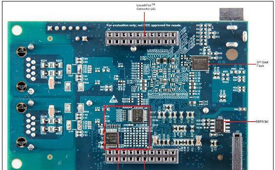
图3.评估板TMDSEVM6670L外形图
评估板TMDSEVM6670L包括:
• TMS320C6678 Evaluation Module
• Power adapter and power cord
• USB cable for on-board JTAG emulation (XDS100v1)
• Ethernet cable
• RS-232 serial cable
• Software (DVD) and documentation
责任编辑:HanFeng
【免责声明】
1、本文内容、数据、图表等来源于网络引用或其他公开资料,版权归属原作者、原发表出处。若版权所有方对本文的引用持有异议,请联系拍明芯城(marketing@iczoom.com),本方将及时处理。
2、本文的引用仅供读者交流学习使用,不涉及商业目的。
3、本文内容仅代表作者观点,拍明芯城不对内容的准确性、可靠性或完整性提供明示或暗示的保证。读者阅读本文后做出的决定或行为,是基于自主意愿和独立判断做出的,请读者明确相关结果。
4、如需转载本方拥有版权的文章,请联系拍明芯城(marketing@iczoom.com)注明“转载原因”。未经允许私自转载拍明芯城将保留追究其法律责任的权利。
拍明芯城拥有对此声明的最终解释权。


 产品分类
产品分类




 2012- 2022 拍明芯城ICZOOM.com 版权所有 客服热线:400-693-8369 (9:00-18:00)


