


 产品分类
产品分类
基于Lattice公司的iCE40 Ultra系列FPGA开发方案
 126
126
 拍明
拍明
原标题:Lattice iCE40 Ultra系列FPGA开发方案
lattice公司的iCE40 Ultra系列是超低功耗FPGA和传感器管理器件,采用先进的40nm超低功耗工艺,集成了能和所有移动传感器和应用处理器接口的SPI和I2C区块, 还集成了10kHz(LFOSC)和48MHz(HFOSC)的片上振荡器,待机电流低至71uA,主要用于智能手机,平板电脑,手持通信设备厂,多传感器管理应用,传感器预处理和传感器融合以及常开传感器应用.本文介绍了iCE40 Ultra系列FPGA主要特性, iCE5LP-4K器件框图和DSP框图, iCE40 Ultra系列FPGA分接板主要特性和框图,电路图和材料清单.
iCE40 Ultra family is an ultra-low power FPGA and sensor manager designed for ultra-low power mobile applications, such as smartphones, tablets and hand-held devices. The iCE40 Ultra family includes integrated SPI and I2C blocks to interface with virtually all mobile sensors and application processors. The iCE40 Ultra family also features two on-chip oscillators, 10 kHz and 48 MHz. The LFOSC (10 kHz) is ideal for low power function in always-on applications , while HFOSC (48 MHz) can be used for awaken activities.
The iCE40 Ultra family also features DSP functional block to off-load Application Processor to pre-process informa-tion sent from the mobile sensors. The embedded RGB PWM IP, with the three 24 mA constant current RGB out-puts on the iCE40 Ultra provides all the necessary logic to directly drive the service LED, without the need of external MOSFET or buffer. The 500 mA constant current IR driver output provides a direct interface to external LED for application such as IrDA functions. Users simply implement the modulation logic that meets his needs, and connect the IR driver directly to the LED, without the need of external MOSFET or buffer. This high current driver can also be used as Barcode Emulation, sending barcode information to external Barcode Reader.
The iCE40 Ultra family of devices are targeting for mobile applications to perform functions such as IrDA, Service LED, Barcode Emulation, GPIO Expander, SDIO Level Shift, and other custom functions. The iCE40 Ultra family features three device densities, from 1100 to 3520 Look Up Tables (LUTs) of logic with pro-grammable I/Os that can be used as either SPI/I2C interface ports or general purpose I/O’s. It also has up to 80 kbits of Block RAMs to work with user logic.
iCE40 Ultra系列FPGA主要特性:
Flexible Logic Architecture
• Three devices with 1100 to 3520 LUTs
• Offered in WLCS package
Ultra-low Power Devices
• Advanced 40 nm ultra-low power process
• As low as 71 μA standby current typical
Embedded Memory
• Up to 80 kbits sysMEM™ Embedded Block RAM
Two Hardened I2C Interfaces
Two Hardened SPI Interfaces
Two On-Chip Oscillators
• Low Frequency Oscillator – 10 kHz
• High Frequency Oscillator – 48 MHz
24 mA Current Drive RGB LED Outputs
• Three drive outputs in each device
• User selectable sink current up to 24 mA
500 mA Current Drive IR LED Output
• One IR drive output in each device
• User selectable sink current up to 500 mA
On-chip DSP
• Signed and unsigned 8-bit or 16-bit functions
• Functions include Multiplier, Accumulator, and Multiply-Accumulate (MAC)
Flexible On-Chip Clocking
• Eight low skew global signal resource, six can be directly driven from external pins
• One PLL with dynamic interface per device
Flexible Device Configuration
• SRAM is configured through:
— Standard SPI Interface
— Internal Nonvolatile Configuration Memory (NVCM)
Ultra-Small Form Factor
• As small as 2.078 mm x 2.078 mm
iCE40 Ultra系列FPGA应用:
• Smartphones
• Tablets and Consumer Handheld Devices
• Handheld Commercial and Industrial Devices
• Multi Sensor Management Applications
• Sensor Pre-processing and Sensor Fusion
• Always-On Sensor Applications
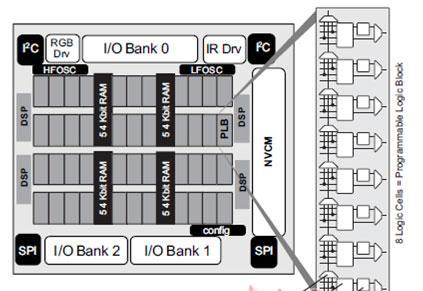
图1.iCE5LP-4K器件框图(顶视图)
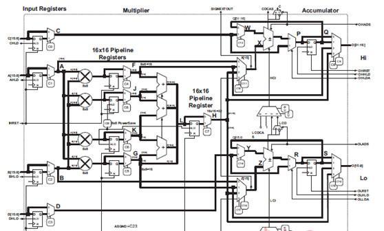
图2. sysDSP 功能框图(16位x16位乘法累加)
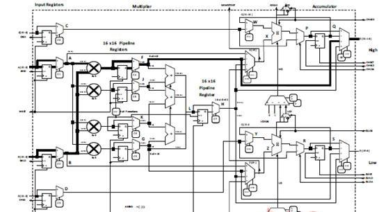
图3. sysDSP 功能框图(8位x8位乘法器)
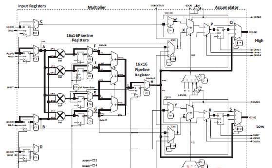
图4. DSP 功能框图(16位x16位乘法器)
iCE40 Ultra系列FPGA分接板
This guide describes how to begin using the iCE40 Ultra Breakout Board, an easy-to-use platform for demonstrating the high-current LED drive capabilities of the iCE40 Ultra FPGA. Along with the evaluation board and accessories, this kit includes the pre-loaded LED Driver Demo that demonstrates driving the RGB LEDs with a PWM circuit. In addition, most of the device’s I/O balls are accessible via one of the several header locations on the board, facilitating rapid prototyping of user functions. The contents of this user’s guide include demo operation, top-level functional descriptions of the various portions of the evaluation board, descriptions of the on-board connectors, shunts, a complete set of schematics and the bill of materials for the iCE40 Ultra Breakout Board. Note: Static electricity can severely shorten the lifespan of electronic components. Be careful when handling the iCE40 Ultra Breakout Board as to not damage it from ESD.
iCE40 Ultra系列FPGA分接板主要特性:
• iCE40 Ultra Breakout Board – The iCE40 Ultra Breakout Board features the following on-board components and circuits:
– iCE40 Ultra (iCE5LP4K-SWG36) device in a 36-ball WLCSP package.
– Example of a board using this 0.35-pitch WLCSP package.
– High-current LED output – Infrared transmit
– iCE40 Ultra Current Measurements
– Standard USB cable for device programming
– RoHS-compliant packaging and process
• Pre-loaded Demo – The kit includes a pre-loaded demo to control the onboard RGB LED in conjunction with a software run GUI.
• USB Connector Cable – A mini B USB port provides power, a programming interface and communication for the software RGB LED GUI to the iCE40 Ultra SPI port.
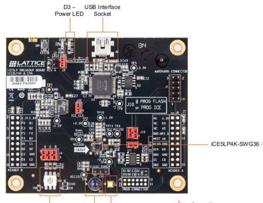
图5. iCE40 Ultra系列FPGA分接板外形图(顶层)
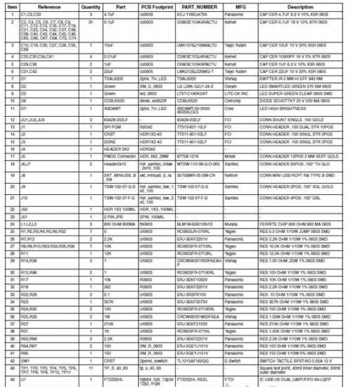
iCE40 Ultra系列FPGA分接板材料清单:
责任编辑:HanFeng
【免责声明】
1、本文内容、数据、图表等来源于网络引用或其他公开资料,版权归属原作者、原发表出处。若版权所有方对本文的引用持有异议,请联系拍明芯城(marketing@iczoom.com),本方将及时处理。
2、本文的引用仅供读者交流学习使用,不涉及商业目的。
3、本文内容仅代表作者观点,拍明芯城不对内容的准确性、可靠性或完整性提供明示或暗示的保证。读者阅读本文后做出的决定或行为,是基于自主意愿和独立判断做出的,请读者明确相关结果。
4、如需转载本方拥有版权的文章,请联系拍明芯城(marketing@iczoom.com)注明“转载原因”。未经允许私自转载拍明芯城将保留追究其法律责任的权利。
拍明芯城拥有对此声明的最终解释权。
相关资讯
:
基于MC33771主控芯片的新能源锂电池管理系统解决方案

AMIC110 32位Sitara ARM MCU开发方案

基于AMIC110多协议可编程工业通信处理器的32位Sitara ARM MCU开发方案

基于展讯SC9820超低成本LTE芯片平台的儿童智能手表解决方案

基于TI公司的AM437x双照相机参考设计

基于MTK6580芯片的W2智能手表解决方案


 2012- 2022 拍明芯城ICZOOM.com 版权所有 客服热线:400-693-8369 (9:00-18:00)


