


 产品分类
产品分类
基于Microchip公司的PIC32MX1系列MCU入门开发方案
 115
115
 拍明
拍明
原标题:Microchip PIC32MX1系列MCU入门开发方案
Microchip公司的PIC32MX12/5系列MCU具有高达83DMIPS的性能,存储器从64/8 KB到512/64 KB 闪存/RAM,用于音频处理和播放的SPI/I2S接口,用于图像和触摸传感接口的并行主端口(PMP)和容性触目惊心传感硬件,以及10位1Msps 48路ADC以及其全速USB2.0器件/主/OTG外设.主要用在工业和汽车电子的CAN通信.本文介绍了PIC32MX1/2/5主要特性和框图,MIPS32® M4K®处理器内核主要特性和框图,以及PIC32MX1/2/5入门开发板特性,电路图,材料清单,PCB元件布局图.
The new PIC32MX1/2 and PIC32MX5 MCU families series boasts a wide variety of additional features, including four SPI/I2S interfaces for audio processing and playback, a Parallel Master Port (PMP) and capacitive touch sensing hardware for graphics and touch-sensing interfaces; a 10-bit, 1 Msps, 48-channel Analog-to-Digital Converter (ADC); as well as a full-speed USB 2.0 Device/Host/OTG peripheral. To maximize data throughput, each MCU includes four general-purpose direct memory access controllers (DMAs) and two dedicated DMAs on each CAN and USB module.
In addition to their rich mix of integrated hardware peripheral features, these MCUs are supported by Microchip’s powerful MPLAB® Harmony software development framework, which simplifies the software development process by integrating the license, resale and support of Microchip and third-party middleware, drivers, libraries and real time operating systems (RTOSs). Specifically, Microchip’s readily available software packages, such as Bluetooth audio development suites, Bluetooth Serial Port Profile library, audio equalizer filter libraries, various Decoders (including AAC, MP3, WMA and SBC), sample-rate conversion libraries, CAN2.0B PLIBs, USB stacks, and graphics libraries can rapidly reduce the development time of applications, including Bluetooth connectivity, digital audio, consumer, industrial, medical and general-purpose embedded control.
PIC32MX1/2/5主要特性:
Operating Conditions
• 2.3V to 3.6V, -40℃ to +105℃, DC to 40 MHz
• 2.3V to 3.6V, -40℃ to +85℃, DC to 50 MHz
Core: 50 MHz/83 DMIPS MIPS32® M4K®
• MIPS16e® mode for up to 40% smaller code size
• Code-efficient (C and Assembly) architecture
• Single-cycle (MAC) 32x16 and two-cycle 32x32 multiply
Clock Management
• 0.9% internal oscillator
• Programmable PLLs and oscillator clock sources
• Fail-Safe Clock Monitor (FSCM)
• Independent Watchdog Timer
• Fast wake-up and start-up
Power Management
• Low-power management modes (Sleep and Idle)
• Integrated Power-on Reset and Brown-out Reset
• 0.5 mA/MHz dynamic current (typical)
• 20 μA IPD current (typical)
Audio Interface Features
• Data communication: I2S, LJ, RJ, and DSP modes
• Control interface: SPI and I2C™
• Master clock:
- Generation of fractional clock frequencies
- Can be synchronized with USB clock
- Can be tuned in run-time
Advanced Analog Features
• ADC Module:
- 10-bit 1.1 Msps rate with one S&H
- Up to 10 analog inputs on 28-pin devices and 13 analog inputs on 44-pin devices
• Flexible and independent ADC trigger sources
• Charge Time Measurement Unit (CTMU):
- Supports mTouch™ capacitive touch sensing
- Provides high-resolution time measurement (1 ns)
- On-chip temperature measurement capability
• Comparators:
- Up to three Analog Comparator modules
- Programmable references with 32 voltage points
Timers/Output Compare/Input Capture
• Five General Purpose Timers:
- Five 16-bit and up to two 32-bit Timers/Counters
• Five Output Compare (OC) modules
• Five Input Capture (IC) modules
• Peripheral Pin Select (PPS) to allow function remap
• Real-Time Clock and Calendar (RTCC) module
Communication Interfaces
• USB 2.0-compliant Full-speed OTG controller
• Two UART modules (12.5 Mbps):
- Supports LIN 2.0 protocols and IrDA® support
• Two 4-wire SPI modules (25 Mbps)
• Two I2C modules (up to 1 Mbaud) with SMBus support
• PPS to allow function remap
• Parallel Master Port (PMP)
Direct Memory Access (DMA)
• Four channels of hardware DMA with automatic data size detection
• Two additional channels dedicated for USB
• Programmable Cyclic Redundancy Check (CRC)
Input/Output
• 10 mA source/sink on all I/O pins and up to 14 mA on
non-standard VOH
• 5V-tolerant pins
• Selectable open drain, pull-ups, and pull-downs
• External interrupts on all I/O pins
Qualification and Class B Support
• AEC-Q100 REVG (Grade 2 -40℃ to +105℃) planned
• Class B Safety Library, IEC 60730
Debugger Development Support
• In-circuit and in-application programming
• 4-wire MIPS® Enhanced JTAG interface
• Unlimited program and six complex data breakpoints
• IEEE 1149.2-compatible (JTAG) boundary scan
The MIPS32® M4K® Processor Core is the heart of the PIC32MX1XX/2XX family processor. The CPU fetches instructions, decodes each instruction, fetches source operands, executes each instruction and writes the results of instruction execution to the destinations The MIPS32 M4K processor core contains several logic blocks working together in parallel, providing an efficient high-performance computing engine. The following blocks are included with the core:
• Execution Unit
• Multiply/Divide Unit (MDU)
• System Control Coprocessor (CP0)
• Fixed Mapping Translation (FMT)
• Dual Internal Bus interfaces
• Power Management
• MIPS16e® Support
• Enhanced JTAG (EJTAG) Controller
MIPS32® M4K®处理器内核主要特性:
• 5-stage pipeline
• 32-bit address and data paths
• MIPS32 Enhanced Architecture (Release 2)
- Multiply-accumulate and multiply-subtract instructions
- Targeted multiply instruction
- Zero/One detect instructions
- WAIT instruction
- Conditional move instructions (MOVN, MOVZ)
- Vectored interrupts
- Programmable exception vector base
- Atomic interrupt enable/disable
- Bit field manipulation instructions
• MIPS16e® code compression
- 16-bit encoding of 32-bit instructions to improve code density
- Special PC-relative instructions for efficient loading of addresses and constants
- SAVE and RESTORE macro instructions for setting up and tearing down stack frames within
subroutines
- Improved support for handling 8 and 16-bit data types
• Simple Fixed Mapping Translation (FMT) mechanism
• Simple dual bus interface
- Independent 32-bit address and data buses
- Transactions can be aborted to improve interrupt latency
• Autonomous multiply/divide unit
- Maximum issue rate of one 32x16 multiply per clock
- Maximum issue rate of one 32x32 multiply every other clock
- Early-in iterative divide. Minimum 11 and maximum 33 clock latency (dividend (rs) sign
extension-dependent)
• Power control
- Minimum frequency: 0 MHz
- Low-Power mode (triggered by WAIT instruction)
- Extensive use of local gated clocks
• EJTAG debug and instruction trace
- Support for single stepping
- Virtual instruction and data address/value
- Breakpoints
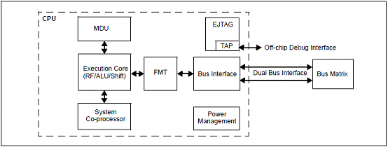
图1. MIPS32® M4K®处理器核框图
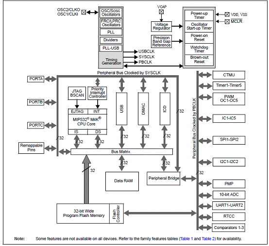
图2.PIC32MX系列框图
PIC32MX1/2/5入门开发板
The PIC32MX1/2/5 Starter Kit provides the user with an easy and cost effective option to experience the USB and CAN functionality of the new PIC32MX1/2/5 family of microcontrollers. The board features a 50MHz/83DMIPS PIC32MX570F512L MCU with 512 KB Flash, 64KB RAM, USB Device/Host/OTG, CAN 2.0B, 48 Channel ADC, Analog Comparators, SPI Ports and UARTs. The starter kit has an onboard high-speed CAN transceiver which serves as an interface between a CAN protocol controller and the physical two wire bus. It also comes equipped with an onboard DB9 connector to interface with the CAN2.0B based applications.
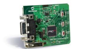
图3. PIC32MX1/2/5入门开发板外形图
PIC32MX1/2/5入门开发板主要特性:
PIC32MX570F512L MCU: 50MHz, 512 KB Flash/64 KB RAM
MCP2562: A High-Speed CAN Transceiver
DB9 Connector for CAN2.0B applications
USB receptacles for USB development
Expansion Connector to interface to PIC32 expansion boards
User definable LEDs & push buttons
Integrated Programmer/Debugger
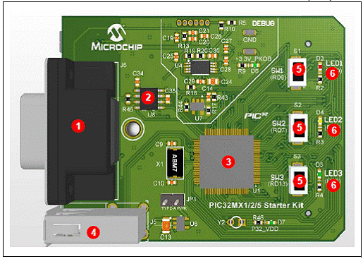
图4. PIC32MX1/2/5入门开发板布局图(顶层)
PIC32MX1/2/5入门开发板布局图(顶层)数字对应元件:
1. DB9 connector for CAN communication (J6).
2. MCP2562 CAN transceiver (U8).
3. PIC32MX570F512L (U1).
4. USB Type A Host connector (J5).
5. User-definable buttons (SW1-SW3).
6. User-definable LEDs (LED1-LED3).
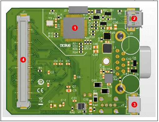
图5. PIC32MX1/2/5入门开发板布局图(底层)
PIC32MX1/2/5入门开发板布局图(顶层)数字对应元件:
1. PIC24FJ256GB106 USB microcontroller for on-board debugging (U2).
2. USB B-mini connector for on-board debugging support (J3).
3. USB micro-AB connector for USB OTG or Device connectivity for PIC32 USB applications (J4).
4. Expansion connector to be used with other Microchip products (J1).
PIC32MX1/2/5入门开发板材料清单:
责任编辑:HanFeng
【免责声明】
1、本文内容、数据、图表等来源于网络引用或其他公开资料,版权归属原作者、原发表出处。若版权所有方对本文的引用持有异议,请联系拍明芯城(marketing@iczoom.com),本方将及时处理。
2、本文的引用仅供读者交流学习使用,不涉及商业目的。
3、本文内容仅代表作者观点,拍明芯城不对内容的准确性、可靠性或完整性提供明示或暗示的保证。读者阅读本文后做出的决定或行为,是基于自主意愿和独立判断做出的,请读者明确相关结果。
4、如需转载本方拥有版权的文章,请联系拍明芯城(marketing@iczoom.com)注明“转载原因”。未经允许私自转载拍明芯城将保留追究其法律责任的权利。
拍明芯城拥有对此声明的最终解释权。
相关资讯
:
基于MC33771主控芯片的新能源锂电池管理系统解决方案

AMIC110 32位Sitara ARM MCU开发方案

基于AMIC110多协议可编程工业通信处理器的32位Sitara ARM MCU开发方案

基于展讯SC9820超低成本LTE芯片平台的儿童智能手表解决方案

基于TI公司的AM437x双照相机参考设计

基于MTK6580芯片的W2智能手表解决方案


 2012- 2022 拍明芯城ICZOOM.com 版权所有 客服热线:400-693-8369 (9:00-18:00)


