


 产品分类
产品分类
基于ST的STM32F303低功耗ARM Cortex-M4 32位MCU开发方案
 511
511
 拍明
拍明
原标题:ST STM32F303低功耗ARM Cortex-M4 32位MCU开发方案
ST公司的STM32F303xB/STM32F303xC系列是基于高性能ARM® Cortex®-M4 32位 RISC内核,其工作频率高达72MHz,器件嵌入了浮点单元(FPU),存储器保护单元(MPU)和嵌入式追踪宏单元(ETM),适用于数字功率,声纳,电机控制,照明和无线充电器等控制敏感应用.本文介绍了STM32F303xB/STM32F303xC主要特性,功能框图, STM32F3DISCOVERY 主要特性,硬件框图,电路图,材料清单,PCB设计文件.
The STM32F303xB/STM32F303xC family is based on the high-performance ARM® Cortex®-M4 32-bit RISC core with FPU operating at a frequency of up to 72 MHz, and embedding a floating point unit (FPU), a memory protection unit (MPU) and an embedded trace macrocell (ETM). The family incorporates high-speed embedded memories (up to 256 Kbytes of Flash memory, up to 40 Kbytes of SRAM) and an extensive range of enhanced I/Os and peripherals connected to two APB buses.
The devices offer up to four fast 12-bit ADCs (5 Msps), seven comparators, four operational amplifiers, up to two DAC channels, a low-power RTC, up to five general-purpose 16-bit timers, one general-purpose 32-bit timer, and two timers dedicated to motor control. They also feature standard and advanced communication interfaces: up to two I2Cs, up to three SPIs (two SPIs are with multiplexed full-duplex I2Ss), three USARTs, up to two UARTs, CAN and USB. To achieve audio class accuracy, the I2S peripherals can be clocked via an external PLL.
The STM32F303xB/STM32F303xC family operates in the -40 to +85 ℃ and -40 to +105 ℃ temperature ranges from a 2.0 to 3.6 V power supply. A comprehensive set of power-saving mode allows the design of low-power applications.
The STM32F303xB/STM32F303xC family offers devices in three packages ranging from 48 pins to 100 pins.
STM32F303xB/STM32F303xC主要特性:
• Core: ARM® Cortex®-M4 32-bit CPU with FPU (72 MHz max), single-cycle multiplication and HW division, 90 DMIPS (from CCM), DSP instruction and MPU (memory protection unit)
• Operating conditions:
– VDD, VDDA voltage range: 2.0 V to 3.6 V
• Memories
– 128 to 256 Kbytes of Flash memory
– Up to 40 Kbytes of SRAM, with HW parity check implemented on the first 16 Kbytes.
– Routine booster: 8 Kbytes of SRAM on instruction and data bus, with HW parity check (CCM)
• CRC calculation unit
• Reset and supply management
– Power-on/Power-down reset (POR/PDR)
– Programmable voltage detector (PVD)
– Low-power modes: Sleep, Stop and Standby
– VBAT supply for RTC and backup registers
• Clock management
– 4 to 32 MHz crystal oscillator
– 32 kHz oscillator for RTC with calibration
– Internal 8 MHz RC with x 16 PLL option
– Internal 40 kHz oscillator
• Up to 87 fast I/Os
– All mappable on external interrupt vectors
– Several 5 V-tolerant
• Interconnect matrix
• 12-channel DMA controller
• Four ADCs 0.20 μS (up to 39 channels) with selectable resolution of 12/10/8/6 bits, 0 to 3.6 V conversion range, single ended/differential input, separate analog supply from 2 to 3.6 V
• Two 12-bit DAC channels with analog supply from 2.4 to 3.6 V
• Seven fast rail-to-rail analog comparators with analog supply from 2 to 3.6 V
• Four operational amplifiers that can be used in PGA mode, all terminals accessible with analog supply from 2.4 to 3.6 V
• Up to 24 capacitive sensing channels supporting touchkey, linear and rotary touch sensors
• Up to 13 timers
– One 32-bit timer and two 16-bit timers with up to 4 IC/OC/PWM or pulse counter and quadrature (incremental) encoder input
– Two 16-bit 6-channel advanced-control timers, with up to 6 PWM channels, deadtime generation and emergency stop – One 16-bit timer with 2 IC/OCs, 1 OCN/PWM, deadtime generation and emergency stop – Two 16-bit timers with IC/OC/OCN/PWM, deadtime generation and emergency stop
– Two watchdog timers (independent, window)
– SysTick timer: 24-bit downcounter
– Two 16-bit basic timers to drive the DAC
• Calendar RTC with Alarm, periodic wakeup from Stop/Standby
• Communication interfaces
– CAN interface (2.0B Active)
– Two I2C Fast mode plus (1 Mbit/s) with 20 mA current sink, SMBus/PMBus, wakeup from STOP
– Up to five USART/UARTs (ISO 7816 interface, LIN, IrDA, modem control)
– Up to three SPIs, two with multiplexed half/full duplex I2S interface, 4 to 16 programmable bit frames – USB 2.0 full speed interface
– Infrared transmitter
• Serial wire debug, Cortex®-M4 with FPU ETM, JTAG
• 96-bit unique ID
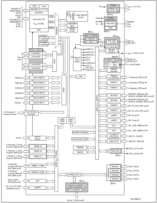
图1. STM32F303xB/STM32F303xC框图
STM32F3DISCOVERY: STM32F303xx MCU Discovery kit
The STM32F3DISCOVERY is designed to help you explore the features of the STM32 F3 32-bit ARM® Cortex™-M4 mixed-signal MCU, and develop your applications. It is based on an STM32F303VCT6 and includes an ST-LINK/V2 embedded debug tool interface, Gyroscope ST MEMS, E-compass with accelerometer ST MEMS, LEDs, pushbuttons and a USB mini-B connector.
T STM32F3DISCOVERY 主要特性:
● STM32F303VCT6 microcontroller featuring 256 KB of Flash memory, 48 KB of RAM in an LQFP100 package.
● On-board ST-LINK/V2 with selection mode switch to use the kit as a standalone ST-LINK/V2 (with SWD connector for programming and debugging).
● Board power supply: through the USB bus or from an external 3 V or 5 V supply voltage.
● External application power supply: 3 V and 5 V.
● L3GD20, ST MEMS motion sensor, 3-axis digital output gyroscope.
● LSM303DLHC, ST MEMS system-in-package featuring a 3D digital linear acceleration sensor and a 3D digital magnetic sensor.
● Ten LEDs:
– LD1 (red) for 3.3 V power-on.
– LD2 (red/green) for USB communication.
– Eight user LEDs, LD3/10 (red), LD4/9 (blue), LD5/8 (orange) and LD6/7 (green).
● Two pushbuttons (user and reset).
● USB USER with Mini-B connector.
● Extension header for LQFP100 I/Os for quick connection to prototyping board and easy probing.

图2. STM32F3DISCOVERY外形图
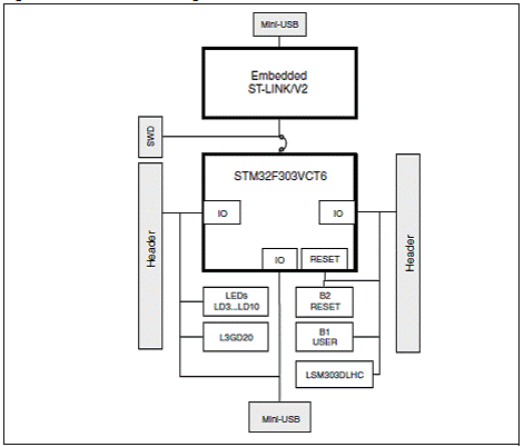
图3. STM32F3DISCOVERY硬件框图
责任编辑:HanFeng
【免责声明】
1、本文内容、数据、图表等来源于网络引用或其他公开资料,版权归属原作者、原发表出处。若版权所有方对本文的引用持有异议,请联系拍明芯城(marketing@iczoom.com),本方将及时处理。
2、本文的引用仅供读者交流学习使用,不涉及商业目的。
3、本文内容仅代表作者观点,拍明芯城不对内容的准确性、可靠性或完整性提供明示或暗示的保证。读者阅读本文后做出的决定或行为,是基于自主意愿和独立判断做出的,请读者明确相关结果。
4、如需转载本方拥有版权的文章,请联系拍明芯城(marketing@iczoom.com)注明“转载原因”。未经允许私自转载拍明芯城将保留追究其法律责任的权利。
拍明芯城拥有对此声明的最终解释权。
相关资讯
:
基于MC33771主控芯片的新能源锂电池管理系统解决方案

AMIC110 32位Sitara ARM MCU开发方案

基于AMIC110多协议可编程工业通信处理器的32位Sitara ARM MCU开发方案

基于展讯SC9820超低成本LTE芯片平台的儿童智能手表解决方案

基于TI公司的AM437x双照相机参考设计

基于MTK6580芯片的W2智能手表解决方案


 2012- 2022 拍明芯城ICZOOM.com 版权所有 客服热线:400-693-8369 (9:00-18:00)


