


 产品分类
产品分类
Microchip PIC16LF171X MCU+RN4020 BLE计步器开发方案
 203
203
 拍明
拍明
原标题:Microchip PIC16LF171X MCU+RN4020 BLE计步器开发方案
Microchip公司的计步器主要采用PIC16LF171X低功耗MCU和低功耗蓝牙模块RN4020 BLE,以及各种传感器,激励器,存储和加密器件等,能测量各种生命信号,能通过智能手机,平板电脑,PC和家庭保健集线器传送医疗机构,存储/发送数据。本文介绍了计步器/可穿戴活动跟踪器开发板主要特性,PIC16LF171X和RN4020 BLE主要特性,计步器演示板框图,固件流程图和电流图.
Wearable fitness and medical devices are becoming an integral part of personal fitness programs and health care delivery. These devices measure a broad range of vital signs, deliver medication, store/transmit data and sync with smartphones, tablets, PCs and home-health hubs. Wearable devices can include many combinations of sensors, actuators, storage and encryption depending on the needs of the user or patient.

图1 计步器应用演示图
The constant struggle to achieve low-power, low-cost and high-performance designs makes the job of the medical or fitness device designer difficult. Microchip Technology’s products address this challenge with extreme low-power capability, effortless connectivity, intelligent analog integration, higher processing power with reduced code size, solid security/authentication capability and innovative touch and input-sensing solutions. Our broad portfolio of products and solutions give designers what they need to create the next generation of wearable devices, including activity trackers, ambulatory ECG recorders, continuous glucose monitors and others that haven’t even been thought about yet.
Low power is a key factor in the design of wearable devices. Microcontollers (MCUs) with low-run currents, multiple low-power sleep modes, flexible wake-up sources and intelligent power management are critical to the success of these designs. Reduced product power consumption enables wearable monitors to use smaller batteries, run longer between re-charging and offer an overall smaller product footprint. Our portfolio of eXtreme Low-Power (XLP) Technology PIC® microcontrollers feature sleep currents as low as 9nA and run currents downto 30 μA/MHz.
计步器/可穿戴活动跟踪器开发板
Pedometer Demonstration/Wearable Activity Tracker Development Board
PIC16LF171X MCU Family/RN4020 Bluetooth® Low Energy Module
This reference demo helps designers develop a low-cost, low-power, wearable pedometer with both an on-board LED display as well as Bluetooth Low Energy capability to connect to smartphones and tablets.*
计步器开发板主要亮点:
Wearable measurement of user step count
Platform for development of more advanced activity tracker functions
LED display is used to demonstrate stand-alone wearable design capability
BTLE module is used to demonstrate smartphone/tablet connected wearable design capability
Low overall BOM cost due to high level of integration
Low-power operation
Uses an eXtreme Low Power PIC16LF1718 MCU
No user motion causes the MCU to go into Sleep mode, wakes up with motion
No user motion causes the Bosch accelerometer to go into low power mode, wakes up with motion
Powered from a single 3V Lithium coin cell battery
Accelerometer uses a step detection firmware library developed by Bosch Sensortec
Additional biometric measurement capability can be added using other Microchip reference designsPedometer Demo。
The Microchip Pedometer Demo can be worn on thewrist like a bracelet/watch. The on-board RN4020 BLEmodule allows the pedometer demo to communicatewith a smartphone or tablet on which the user’sexercise progress can be tracked. The pedometerdemo is powered by a single 3V coin lithium battery(CR2032).
The Microchip pedometer demo uses a Bosch 10-bittriaxial digital accelerometer (BMA250E) to detect themotion of the wearer. The Microchip pedometer demofirmware running in the PIC16LF1718 microcontrollercontains a step detection algorithm library developedby Bosch Sensortec.
A step detection function in this library is calledperiodically by the user application. The microcontrollerwill read the acceleration data of X/Y/Z axes from theaccelerometer via an I2C™ interface when the stepdetection function is called. The step detection functionthen analyzes the accumulated acceleration data anddetermines the number of steps taken by using patternrecognition.
The accumulated number of steps can be shown on thethree digit 7-Segment LED displays or a BLEapplication running in a smartphone/tablet that ispaired with the RN4020 BLE module.
Bluetooth Low Energy (BLE)Communication
The RN4020 BLE module complies with BluetoothCore Specification v4.1. The RN4020 supports 13public profiles and 17 public services based on theGeneric Attribute Profile (GATT). Among supportedpublic profiles, four are health-device-related profiles:
heart rate monitor, health thermometer, glucose meterand blood pressure monitor.
The RN4020 also supports a user-defined privateprofile/service, which can precisely fit a user’sparticular application. This demo defined a privateservice for the pedometer application. Allconfigurations are saved in the on-board non-volatilememory (NVM) of the RN4020, so users need to set upthe module only once.
The microcontroller activates the RN4020 when theBLE communication is enabled by pressing the onboardpush button. The RN4020 then becomespairable with a smartphone or tablet that supports BLE.
The microcontroller periodically sends the step numberto the RN4020 via UART interface after successfulpairing. The RN4020 then transmits the step number tothe paired smartphone or tablet, where a compatibleBLE application can be used to display the step number.
Because the Apple® HealthKit, a new feature for iOS 8,adheres to the BLE GATT specifications, medicaldevices like heart rate and blood pressure monitors,thermometers, and glucose meters that are built withRN4020 will be supported natively by HealthKit. Thatmeans device manufacturers could potentially skip theprocess of developing a companion application for theirproduct, and instead, allow HealthKit to automaticallycontrol the device/accessory itself when it has beenpaired with the RN4020 BLE module.
Human Interface A single push button provides quick function control tothe pedometer demo via the Interrupt-On-Change(IOC) interface.
To turn on/off the LED display, press the button andquickly release it within 1 second.
To enable/disable BLE communication, press thebutton and hold it down for more than 1 second but lessthan 4 seconds.
To zero the step number, press the button and hold itdown for more than 4 seconds, then release it.Power The pedometer demo is powered by a single 3V coinlithium battery (CR2032). The LED displays areautomatically turned off after 10 seconds to savepower.
The baud rate of the UART communication is set to2400 Kbps so that the RN4020 BLE module can remainin Deep Sleep mode when there is no UART datacommunication.
If there is no motion for 16 seconds, the microcontrollerwill get a no-motion interrupt from the accelerometervia the IOC interface. When the no-motion interruptoccurs, the microcontroller reconfigures theaccelerometer to high-g interrupt and then puts it intoLow Power Mode 1. The microcontroller next goes intoSleep mode as well, putting the overall system into thelowest power consumption mode.
In Low Power Mode 1, the accelerometer is periodicallyswitching between a sleep phase and a wake-upphase. During the sleep phase the whole analog circuitof the accelerometer is powered down. During thewake-up phase, the accelerometer works normally andthe high-g interrupt function is running to determinewhen to wake up from the Low Power Mode.
The accelerometer will generate a high-g interrupt towake up the microcontroller when the wearer’s motionis over the preset threshold for a high-accelerationevent, such as walking, picking up the pedometer, orwaving or rotating the pedometer in the air. The pedometer then resumes normal operation afterwaking up.

图2 计步器演示板外形图
Wearable activity trackers featuring step counting and Bluetooth Low Energy (BTLE) have become popular as everyday exercise measurement and motivation tools for people wanting to increase their physical activity and improve their health. Microchip’s Pedometer Demonstration Board is a basic wearable activity tracker that counts each step a person takes by detecting the motion of the person’s body using an accelerometer. It can be worn on the wrist like a bracelet or a watch. Microchip’s Pedometer Demonstration board can also be used as a development platform for the design of more advanced activity tracker functions. The on-board RN4020 BTLE module allows the pedometer to communicate with a smartphone or tablet where the user’s exercise progress can be tracked. The Pedometer Demonstration Board is powered by a single 3V Lithium coin cell battery.
Microchip’s Pedometer Demonstration Board demonstrates the implementation of a Bluetooth Low Energy digital pedometer using Microchip’s PIC16LF1718—a cost- effective 8-bit microcontroller with eXtreme Low Power (XLP) technology, Microchip’s RN4020 Bluetooth 4.1 Low Energy Module and Bosch Sensortec’s BMA250E Digital Triaxial Accelerometer.
计步器演示板主要元件介绍:
PIC16LF1718 MCU
PIC16(L)F1717/8/9 microcontrollers combine Intelligent Analog integration with low cost and extreme low power (XLP)to suit a variety of general purpose applications. These 28-pin and 40-pin devices deliver on-chip op amps, CoreIndependent Peripherals (CLC, NCO and COG), Peripheral Pin Select and Zero-Cross Detect, providing for increased
design flexibility.
Core Features:
• C Compiler Optimized RISC Architecture
• Only 49 Instructions
• Operating Speed:
- 0-32 MHz clock input
- 125 ns minimum instruction cycle
• Interrupt Capability
• 16-Level Deep Hardware Stack
• Up to Four 8-Bit Timers
• One 16-Bit Timer
• Power-on Reset (POR)
• Power-up Timer (PWRT)
• Low-Power Brown-Out Reset (LPBOR)
• Programmable Watchdog Timer (WDT) up to256s
• Programmable Code Protection
Memory:
• Up to 16 Kwords Flash Program Memory
• Up to 2048 Bytes Data SRAM Memory
• Direct, Indirect and Relative Addressing modes
Operating Characteristics:
• Operating Voltage Range:
- 1.8V to 3.6V (PIC16LF1717/8/9)
- 2.3V to 5.5V (PIC16F1717/8/9)
• Temperature Range:
- Industrial: -40°C to 85°C
- Extended: -40°C to 125°C
eXtreme Low-Power (XLP) Features:
• Sleep mode: 50 nA @ 1.8V, typical
• Watchdog Timer: 500 nA @ 1.8V, typical
• Secondary Oscillator: 500 nA @ 32 kHz
• Operating Current:
- 8 uA @ 32 kHz, 1.8V, typical
- 32 uA/MHz @ 1.8V, typical
Digital Peripherals:
• Configurable Logic Cell (CLC):
- Integrated combinational and sequential logic
• Complementary Output Generator (COG):
- Rising/falling edge dead-band control/blanking
• Numerically Controlled Oscillator (NCO):
- Generates true linear frequency control andincreased frequency resolution
- Input Clock: 0 Hz < FNCO < 32 MHz
- Resolution: FNCO/220
• Capture/Compare/PWM (CCP) module
• PWM: Two 10-Bit Pulse-Width Modulators
• Serial Communications:
- SPI, I2C™, RS-232, RS-485, LIN compatible
- Auto-Baud Detect, auto-wake-up on start
• Up to 35 I/O Pins and One Input Pin:
- Individually programmable pull-ups
- Slew rate control
- Interrupt-on-change with edge-select
• Peripheral Pin Select (PPS):
- Enables pin mapping of digital I/O
Intelligent Analog Peripherals:
• Operational Amplifiers:
- Two configurable rail-to-rail op amps
- Selectable internal and external channels
- 2 MHz gain bandwidth product
• High-Speed Comparators:
- Up to two comparators
- 50 ns response time
- Rail-to-rail inputs
• 10-Bit Analog-to-Digital Converter (ADC):
- Up to 28 external channels
- Conversion available during Sleep
- Temperature indicator
• Zero-Cross Detector (ZCD):
- Detect when AC signal on pin crossesground
• 8-Bit Digital-to-Analog Converter (DAC):
- Output available externally
- Internal connections to comparators, opamps, Fixed Voltage Reference (FVR) andADC
• Internal Voltage Reference module
Clocking Structure:
• 16 MHz Internal Oscillator Block:
- ±1% at calibration
- Selectable frequency range from 0 to 32 MHz
• 31 kHz Low-Power Internal Oscillator
• External Oscillator Block with:
- Three crystal/resonator modes up to 20 MHz
- Two external clock modes up to 20 MHz
• Fail-Safe Clock Monitor
• Two-Speed Oscillator Start-up
• Oscillator Start-up Timer (OST)
Programming/Debug Features:
• In-Circuit Debug Integrated On-Chip
• Emulation Header for Advanced Debug:
- Provides trace, background debug and up to32 hardware break points
• In-Circuit Serial Programming™ (ICSP™) via TwoPins
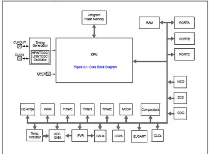
图3 PIC16(L)F1718 MCU框图
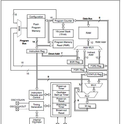
图4 PIC16(L)F1718 MCU内核裁框图
RN4020 BTLE 模块
Microchip’s RN4020 Bluetooth Low Energy Moduleprovides a highly integrated solution for delivering lowpower Bluetooth 4.1 solutions. The advanced commandinterface offers rapid time to market.
The RN4020 module complies with Bluetooth specificationversion 4.1. It integrates RF, a baseband controller,command API processor, making it a completeBluetooth Low Energy Solution.
The RN4020 can be used with either low cost microcontrollerfor intelligent Bluetooth Low Energy applications.
For simple sensor applications, the RN4020internal scripting capabilities enable basic functions tobe implemented without the need for external hostMCU or software development tools.
RN4020 BTLE 模块主要特性:
• Fully qualified Bluetooth® version 4.1 module
• Onboard Bluetooth Low Energy 4.1 stack
• ASCII command interface API over UART
• Compact form factor 11.5 x 19.5 x 2.5 mm
• Castellated SMT pads for easy and reliable PCBmounting
• Environmentally friendly, RoHS compliant
• Certifications: FCC, IC, CE, QDID
• Device Firmware Upgrade (DFU) over UART orOver the Air (OTA)
• Microchip Low-energy Data Profile (MLDP) forserial data applications
• Remote commands over the air
Operational
• Single operating voltage: 3.0V to 3.6V (3.3V typical)
• Temperature range: -30℃ to 85℃
• Low-power consumption
• Simple, UART interface
• Integrated Crystal, Internal Voltage Regulator,Matching Circuitry, Memory Amplifier, and PCBAntenna
• Multiple IOs for control and status
• UART interface, GPIO, ADC
• 64 KB internal serial flash
RF/Analog Features
• ISM Band 2.402 to 2.480 GHz operation
• Channels 0-39
• Rx Sensitivity: -92.5 dBm at 0.1% BER
• Tx Power: +7 dBm
• RSSI monitor
MAC/Baseband/Higher Layer Features
• Secure AES128 encryption
• GAP, GATT, SM, L2CAP and integrated publicprofiles
• Create custom services using command API
• Keyboard I/O Authentication
• Software configurable role as peripheral or central,client or server
RN4020 BTLE 模块应用:
• Health/Medical Devices
- Glucose Meters
- Heart rate
- Scale
• Sports Activity and Fitness
- Pedometer
- Cycling computer
- Heart rate
• Retail
- POS
- Asset tagging and tracking
- Proximity Advertising
• Beacon applications
• Internet of Things Sensor tag
• Remote Control
- Keyboard Mice
- AV consoles, game controllers
• Wearable smart devices and accessories
• Industrial Control
- Private (custom) services
- Low bandwidth cable replacement
Smart Energy/Smart Home
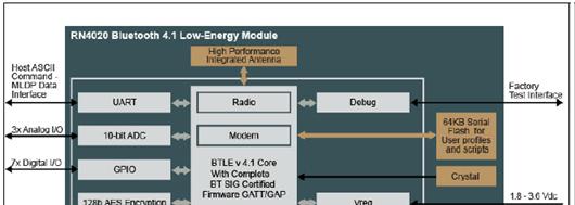
图5 RN4020框图
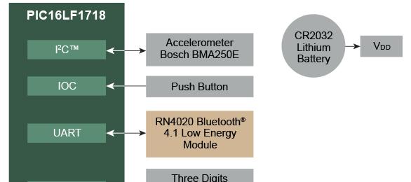
图6 计步器演示板框图
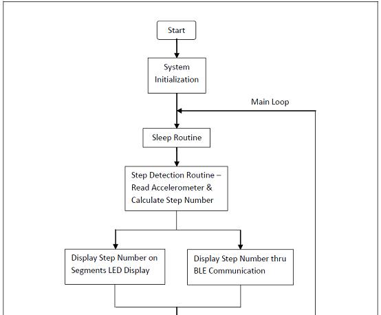
图7 计步器演示板固件流程图
责任编辑:HanFeng
【免责声明】
1、本文内容、数据、图表等来源于网络引用或其他公开资料,版权归属原作者、原发表出处。若版权所有方对本文的引用持有异议,请联系拍明芯城(marketing@iczoom.com),本方将及时处理。
2、本文的引用仅供读者交流学习使用,不涉及商业目的。
3、本文内容仅代表作者观点,拍明芯城不对内容的准确性、可靠性或完整性提供明示或暗示的保证。读者阅读本文后做出的决定或行为,是基于自主意愿和独立判断做出的,请读者明确相关结果。
4、如需转载本方拥有版权的文章,请联系拍明芯城(marketing@iczoom.com)注明“转载原因”。未经允许私自转载拍明芯城将保留追究其法律责任的权利。
拍明芯城拥有对此声明的最终解释权。
相关资讯
:
基于MC33771主控芯片的新能源锂电池管理系统解决方案

AMIC110 32位Sitara ARM MCU开发方案

基于AMIC110多协议可编程工业通信处理器的32位Sitara ARM MCU开发方案

基于展讯SC9820超低成本LTE芯片平台的儿童智能手表解决方案

基于TI公司的AM437x双照相机参考设计

基于MTK6580芯片的W2智能手表解决方案


 2012- 2022 拍明芯城ICZOOM.com 版权所有 客服热线:400-693-8369 (9:00-18:00)


