基于ST STM32F103CBU6T+TI CC1101 RF芯片的烟感火灾探测报警器解决方案
 777
777
 拍明
拍明
原标题:联合捷迅易联推出基于 ST STM32FCBT6 烟感火灾探测报警器
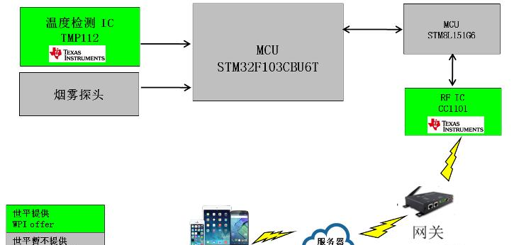
世平集团联合深圳捷迅易联有限公司推出基于 ST STM32FCBT6 的物联网烟感火灾探测报警器,该技术在传统烟感功能上增加了无线射频功能。无线数据通过网关、服务器,将火警通知第一时间告知住户业主及管理处。方案的无线传输部分采用了 TI CC1101 RF 芯片实现。CC1101 是低功耗低于 1GHz 的收发器,专为非常低功耗的无线应用而设计。 该芯片主要用于 315,433,868 和 915 MHz 的 ISM(工业,科学和医疗)和 SRD(短距离设备)频段。
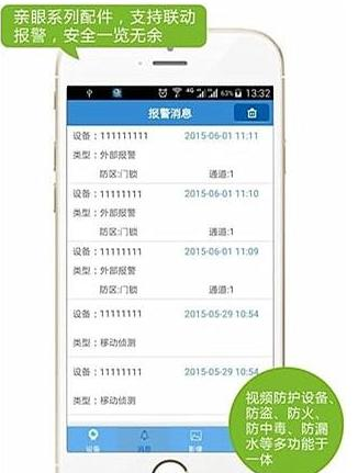
场景应用图

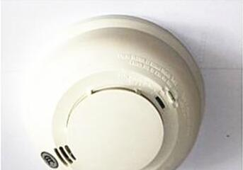
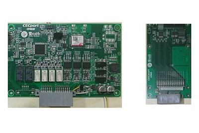
产品实体图
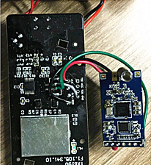
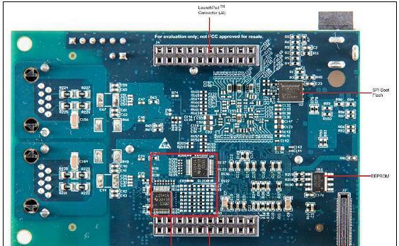
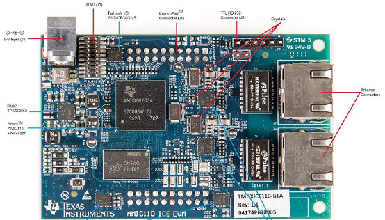
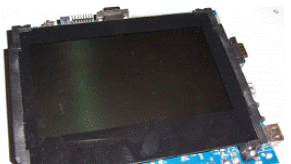
展示板照片
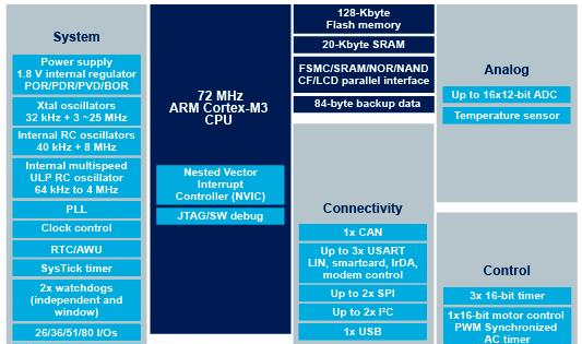
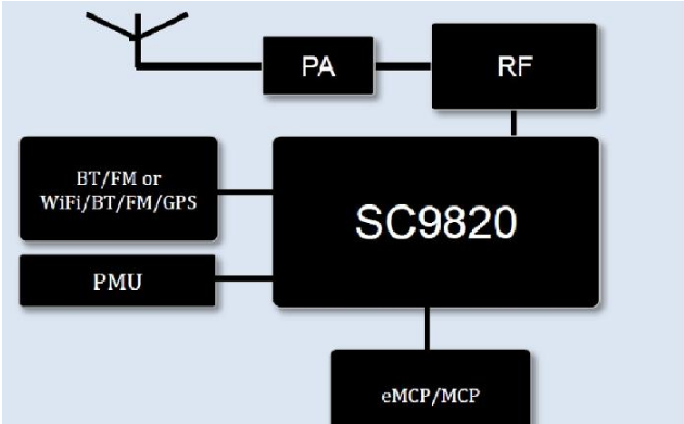
方案方块图
核心技术优势
1. 物联网烟感火灾探测报警器
2. 报警通知可无线传输、实时监测
3. 云端连接,可实现远程监控
方案规格
1. 72 MHz的32位ARM Cortex-M4内核
2. 1μs的双12位ADC,4兆位/秒的UART,18兆位/秒的SPI
3. 片上集成32-512KB的Flash存储器。6-64KB的SRAM存储器
4. TI CC1101 RF 芯片实现低功耗无线传输
5. 性价比高、配置丰富灵活、低功耗
6. 出色的实时性能
【STM32F103CB】
Mainstream Performance line, ARM Cortex-M3 MCU with 128 Kbytes Flash, 72 MHz CPU, motor control, USB and CAN
The STM32F103xx medium-density performance line family incorporates the high-performance ARM®Cortex®-M3 32-bit RISC core operating at a 72 MHz frequency, high-speed embedded memories (Flash memory up to 128 Kbytes and SRAM up to 20 Kbytes), and an extensive range of enhanced I/Os and peripherals connected to two APB buses. All devices offer two 12-bit ADCs, three general purpose 16-bit timers plus one PWM timer, as well as standard and advanced communication interfaces: up to two I2Cs and SPIs, three USARTs, an USB and a CAN.
The devices operate from a 2.0 to 3.6 V power supply. They are available in both the –40 to +85 °C temperature range and the –40 to +105 °C extended temperature range. A comprehensive set of power-saving mode allows the design of low-power applications.
The STM32F103xx medium-density performance line family includes devices in six different package types: from 36 pins to 100 pins. Depending on the device chosen, different sets of peripherals are included, the description below gives an overview of the complete range of peripherals proposed in this family.
These features make the STM32F103xx medium-density performance line microcontroller family suitable for a wide range of applications such as motor drives, application control, medical and handheld equipment, PC and gaming peripherals, GPS platforms, industrial applications, PLCs, inverters, printers, scanners, alarm systems, video intercoms, and HVACs.
Key Features
ARM®32-bit Cortex®-M3 CPU Core
72 MHz maximum frequency,1.25 DMIPS/MHz (Dhrystone 2.1) performance at 0 wait state memory access
Single-cycle multiplication and hardware division
Memories
64 or 128 Kbytes of Flash memory
20 Kbytes of SRAM
Clock, reset and supply management
2.0 to 3.6 V application supply and I/Os
POR, PDR, and programmable voltage detector (PVD)
4-to-16 MHz crystal oscillator
Internal 8 MHz factory-trimmed RC
Internal 40 kHz RC
PLL for CPU clock
32 kHz oscillator for RTC with calibration
Low-power
Sleep, Stop and Standby modes
VBAT supply for RTC and backup registers
2 x 12-bit, 1 μs A/D converters (up to 16 channels)
Conversion range: 0 to 3.6 V
Dual-sample and hold capability
Temperature sensor
DMA
7-channel DMA controller
Peripherals supported: timers, ADC, SPIs, I2Cs and USARTs
Up to 80 fast I/O ports
26/37/51/80 I/Os, all mappable on 16 external interrupt vectors and almost all 5 V-tolerant
Debug mode
Serial wire debug (SWD) & JTAG interfaces
7 timers
Three 16-bit timers, each with up to 4 IC/OC/PWM or pulse counter and quadrature (incremental) encoder input
16-bit, motor control PWM timer with dead-time generation and emergency stop
2 watchdog timers (Independent and Window)
SysTick timer 24-bit downcounter
Up to 9 communication interfaces
Up to 2 x I2C interfaces (SMBus/PMBus)
Up to 3 USARTs (ISO 7816 interface, LIN, IrDA capability, modem control)
Up to 2 SPIs (18 Mbit/s)
CAN interface (2.0B Active)
USB 2.0 full-speed interface
CRC calculation unit, 96-bit unique ID
Packages are ECOPACK®
CIRCUIT DIAGRAM
【CC1101】
低功耗(低于 1GHz)射频收发器

描述
CC1101 is a low-cost sub-1 GHz transceiver designed for very low-power wireless applications. The circuit is mainly intended for the ISM (Industrial, Scientific and Medical) and SRD (Short Range Device) frequency bands at 315, 433, 868, and 915 MHz, but can easily be programmed for operation at other frequencies in the 300-348 MHz, 387-464 MHz and 779-928 MHz bands.
The RF transceiver is integrated with a highly configurable baseband modem. The modem supports various modulation formats and has a configurable data rate up to 600 kbps.
CC1101 provides extensive hardware support for packet handling, data buffering, burst transmissions, clear channel assessment, link quality indication, and wake-on-radio.
The main operating parameters and the 64- byte transmit/receive FIFOs of CC1101 can be controlled via an SPI interface. In a typical system, the CC1101 will be used together with a microcontroller and a few additional passive components.
The CC1190 850-950 MHz range extender [21] can be used with CC1101 in long range applications for improved sensitivity and higher output power.
特性
RF Performance
High sensitivity
–116 dBm at 0.6 kBaud, 433 MHz, 1% packet error rate
–112 dBm at 1.2 kBaud, 868 MHz, 1% packet error rate
Low current consumption (14.7 mA in RX, 1.2 kBaud, 868 MHz)
Programmable output power up to +12 dBm for all supported frequencies
Excellent receiver selectivity and blocking performance
Programmable data rate from 0.6 to 600 kbps
Frequency bands: 300-348 MHz, 387-464 MHz and 779-928 MHz
Analog Features
2-FSK, 4-FSK, GFSK, and MSK supported as well as OOK
and flexible ASK shaping
Suitable for frequency hopping systems due to a fast settling
frequency synthesizer; 75 µs settling time
Automatic Frequency Compensation (AFC) can be used to align the frequency
synthesizer to the received signal centre frequency
Integrated analog temperature sensor
Digital Features
Flexible support for packet oriented systems; On-chip support for
sync word detection, address check, flexible packet length, and
automatic CRC handling
Efficient SPI interface; All registers can be programmed with
one "burst" transfer
Digital RSSI output
Programmable channel filter bandwidth
Programmable Carrier Sense (CS) indicator
Programmable Preamble Quality Indicator (PQI) for improved protection
against false sync word detection in random noise
Support for automatic Clear Channel Assessment (CCA) before transmitting
(for listen-before-talk systems)
Support for per-package Link Quality Indication (LQI)
Optional automatic whitening and de-whitening of data
Low-Power Features
200 nA sleep mode current consumption
Fast startup time; 240 µs from sleep to RX or TX
mode (measured on EM reference design [1] and [2])
Wake-on-radio functionality for automatic low-power RX polling
Separate 64-byte RX and TX data FIFOs (enables burst mode data transmission)
General
Few external components; Completely on-chip frequency synthesizer, no external
filters or RF switch needed
Green package: RoHS compliant and no antimony or bromine
Small size (QLP 4x4 mm package, 20 pins)
Suited for systems targeting compliance with EN 300 220 (Europe) and
FCC CFR Part 15 (US)
Suited for systems targeting compliance with the Wireless MBUS standard EN 13757-4:2005
Support for asynchronous and synchronous serial receive/transmit mode for backwards
compatibility with existing radio communication protocols
Improved Range using CC1190
The CC1190 [21] is a range extender for 850-950 MHz and is an ideal
fit for CC1101 to enhance RF performance
High sensitivity–118 dBm at 1.2 kBaud, 868 MHz, 1% packet error
rate–120 dBm at 1.2 kBaud, 915 MHz, 1% packet error rate
+20 dBm output power at 868 MHz
+27 dBm output power at 915 MHz
Refer to AN094 [22] and AN096 [23] for more performance figures of the
CC1101 + CC1190 combination
Reduced Battery Current using TPS62730
The TPS62730 [26] is a step down converter with bypass mode for
ultra low power wireless applications
In RX, the current drawn from a 3.6 V battery is typically less than
11 mA when TPS62730 output voltage is 2.1 V. When connecting CC1101
directly to a 3.6 V battery the current drawn is typically 17 mA
In TX, at maximum output power (+12 dBm), the current drawn from a
3.6 V battery is typically 22 mA when TPS62730 output voltage is 2.1 V.
When connecting CC1101 directly to a 3.6 V battery the current drawn is
typically 34 mA
When CC1101 enters SLEEP mode, the TPS62730 can be put
in bypass mode for very low power down current
The typical TPS62730 current consumption is 30 nA in bypass mode.
The CC1101 is connected to the battery via an integrated 2.1 Ω (typical)
switch in bypass mode
责任编辑:David
【免责声明】
1、本文内容、数据、图表等来源于网络引用或其他公开资料,版权归属原作者、原发表出处。若版权所有方对本文的引用持有异议,请联系拍明芯城(marketing@iczoom.com),本方将及时处理。
2、本文的引用仅供读者交流学习使用,不涉及商业目的。
3、本文内容仅代表作者观点,拍明芯城不对内容的准确性、可靠性或完整性提供明示或暗示的保证。读者阅读本文后做出的决定或行为,是基于自主意愿和独立判断做出的,请读者明确相关结果。
4、如需转载本方拥有版权的文章,请联系拍明芯城(marketing@iczoom.com)注明“转载原因”。未经允许私自转载拍明芯城将保留追究其法律责任的权利。
拍明芯城拥有对此声明的最终解释权。


 产品分类
产品分类




 2012- 2022 拍明芯城ICZOOM.com 版权所有 客服热线:400-693-8369 (9:00-18:00)


