


 产品分类
产品分类
基于TI公司的TIDA-00446小型强隔离三相逆变器IGBT栅驱动参考设计
 167
167
 拍明
拍明
原标题:TI TIDA-00446小型强隔离三相逆变器IGBT栅驱动参考设计
TI公司的TIDA-00446是采用ISO5851的小型强隔离三相逆变器IGBT栅驱动参考设计,包括有六个强隔离IGBT栅驱动器,用来控制三相逆变器如AC驱动,UPS和太阳能逆变器的IGBT,适用于低压驱动如400Vac和690Vac ,可驱动电流高达50A的IGBT模块,主要用在变速驱动,UPS,太阳能逆变器和焊接机.本文介绍了ISO5851主要特性,框图,典型马达驱动框图以及TIDA-00446三相逆变器参考设计主要特性,框图,电路图,材料清单和PCB设计图.
The ISO5851 is a 5.7-kVRMS, reinforced isolated gate driver for IGBTs and MOSFETs with 2.5-A source and 5-A sink current. The input side operates from a single 3-V to 5.5-V supply. The output side allows for a supply range from minimum 15-V to maximum 30-V. Two complementary CMOS inputs control the output state of the gate driver. The short propagation time of 76 ns assures accurate control of the output stage.
An internal desaturation (DESAT) fault detection recognizes when the IGBT is in an overload condition. Upon a DESAT detect the gate driver output is driven low to VEE2 potential turning the IGBT immediately off.
When desaturation is active, a fault signal is sent across the isolation barrier pulling the FLT output at the input side low and blocking the isolator input. The FLT output condition is latched and can be reset through a low-active pulse at the RST input.
When the IGBT is turned off during normal operation with bipolar output supply, the output is hard clamp to VEE2. If the output supply is unipolar, an active Miller clamp can be used, allowing Miller current to sink across a low impedance path preventing IGBT to be dynamically turned on during high voltage transient conditions.
The readiness for the gate driver to be operated is under the control of two undervoltage-lockout circuits monitoring the input side and output side supplies. If either side has insufficient supply the RDY output goes low, otherwise this output is high.
The ISO5851 is available in a 16-pin SOIC package. Device operation is specified over a temperature range from –40℃ to 125℃ ambient.
ISO5851主要特性:
2.5-A Peak Source and 5-A Peak Sink Currents
Short Propagation Delay: 76 ns (Typ), 110 ns (Max)
2-A Active Miller Clamp
Output Short-Circuit Clamp
Fault Alarm upon Desaturation Detection is Signaled on FLT and Reset Through RST
Input and Output Under Voltage Lock-Out (UVLO) with Ready (RDY) Pin Indication
Active Output Pull-down and Default Low Outputs with Low Supply or Floating Inputs
3-V to 5.5-V Input Supply Voltage
15-V to 30-V Output Driver Supply Voltage
CMOS Compatible Inputs
Rejects Input Pulses and Noise Transients
Shorter Than 20 ns
100-kV/µs Minimum Common-Mode Transient Immunity (CMTI) at VCM = 1500 V
Operating Temperature: –40℃ to 125℃ Ambient
Safety and Regulatory Approvals:
8000-VPK VIOTM and 2121-VPK VIORM Reinforced Isolation per DIN V VDE V 0884-10 (VDE V 0884-10):2006-12
5700-VRMS Isolation for 1 Minute per UL 1577
CSA Component Acceptance Notice 5A, IEC 60950-1, IEC 60601-1 and IEC 61010-1 End Equipment Standards
CQC Certification per GB4943.1-2011
All Certifications are Planned
ISO5851主要应用:
Isolated IGBT and MOSFET Drives in
Industrial Motor Control Drives
Industrial Power Supplies
Solar Inverters
HEV and EV Power Modules
Induction Heating
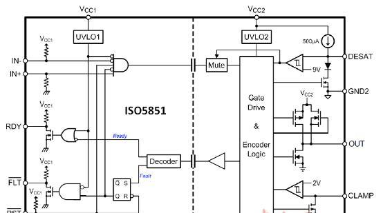
图1.ISO5851框图
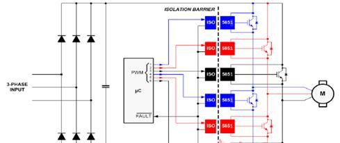
图2.ISO5851典型马达驱动框图
TIDA-00446三相逆变器参考设计
The TIDA-00446 reference design consists of six reinforced isolated IGBT gate drivers along with dedicated gate drive power supplies. This compact reference design is intended to control IGBT’s in 3-phase inverters like AC drives, uninterruptible power supplies (UPS) and solar inverters. The design uses a reinforced isolated IGBT gate driver with DESAT feature and built-in miller clamp protection, enabling use of unipolar supply voltage for the gate drive. Open loop push pull topology based power supply for each gate driver provides flexibility in PCB routing. The push pull transformer driver used in TIDA-00446 operates at 420 khz which helps in reducing the size of the isolation transformer leading to compact power supply solution. Gate drive power supply can be disabled to facilitate safe torque off (STO).
The TIDA-00446 board consists of two main circuit blocks: the isolated gate driver (ISO5851) and the isolated power supply (SN6505 & Transformer) for the gate drive. The primary side of the gate driver is powered from 3.3 V power supply and the secondary, high voltage side is powered from a 17 V isolated power supply. The 17 V isolated supply is derived from a 5 V input rail with the help of a push-pull converter. The converter uses the SN6505B push-pull transformer to drive a center tapped transformer to generate an isolated power supply rail.
A 3-phase inverter has six IGBT switches, so the gate drive section is replicated six times in the board. An individual gate drive and isolated power supply per switch helps achieve a distributed architecture, which increases the flexibility of the PCB layout.
The board has eight control signals consisting of six PWM signals, a reset signal, and an enable signal. The board also provides two monitor signals: the fault and the ready signal. All signals are brought out to a two-row, six-column (2 × 6) berg stick connector and can connect to a 3.3 V powered microcontroller.
The fault signal is an open-drain, active-low signal from the gate driver, which indicates a short circuit in the associated power switch. All six fault signals are logic ANDed together and the resultant signal is made available on the connector. The ready signal is an open-drain power-good signal, which turns active-high when both the primary and secondary power supplies of the gate driver are good. All six ready signals are also logic ANDed together, with the resultant signal made available on the connector. The enable signal disables SN6505. When the enable signal is high all the power supplies are turned off and the board input power reduces to 1 mW. The reset signal reset the fault latch. A 800 ns low pulse is required to reset the fault latches. The enable and reset signal are common to all the gate drivers.
TPS70633 LDO is used to generate a 3.3-V rail from a 5-V input rail for the primary side of the isolated gate drivers. On drive boards where a 3.3-V rail is available, skip this LDO.
TIDA-00446三相逆变器参考设计主要特性:
Suited for low voltage drives (400 Vac and 690 Vac)
Integrated 2.5A source and 5A sink current suits driving IGBT modules with currents up to 50A
Built in miller clamp functionality enables use of unipolar supply voltage (+17 V) for driving IGBT
Built in protection functionalities
Short circuit protection through DESAT detection
Supply Undervoltage protection
Provision for separate Rg(ON) and Rg(OFF)
8000 Vpk Reinforced Isolation
Very high CMTI of > 100 kV/us
Spread spectrum operation of transformer driver helps reduce EMI.
PWM and fault signals of gate drivers can be directly interfaced to controller (3.3V operation)
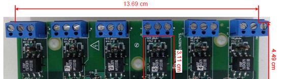
图3.TIDA-00446三相逆变器参考设计外形图
TIDA-00446三相逆变器参考设计设计应用:
• Variable Speed Drives
• UPS
• Solar Inverters
• Welding Machines
TIDA-00446三相逆变器参考设计主要指标:

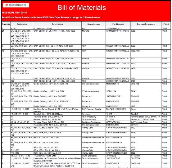
TIDA-00446三相逆变器参考设计材料清单(BOM):
责任编辑:HanFeng
【免责声明】
1、本文内容、数据、图表等来源于网络引用或其他公开资料,版权归属原作者、原发表出处。若版权所有方对本文的引用持有异议,请联系拍明芯城(marketing@iczoom.com),本方将及时处理。
2、本文的引用仅供读者交流学习使用,不涉及商业目的。
3、本文内容仅代表作者观点,拍明芯城不对内容的准确性、可靠性或完整性提供明示或暗示的保证。读者阅读本文后做出的决定或行为,是基于自主意愿和独立判断做出的,请读者明确相关结果。
4、如需转载本方拥有版权的文章,请联系拍明芯城(marketing@iczoom.com)注明“转载原因”。未经允许私自转载拍明芯城将保留追究其法律责任的权利。
拍明芯城拥有对此声明的最终解释权。
相关资讯
:
基于MC33771主控芯片的新能源锂电池管理系统解决方案

AMIC110 32位Sitara ARM MCU开发方案

基于AMIC110多协议可编程工业通信处理器的32位Sitara ARM MCU开发方案

基于展讯SC9820超低成本LTE芯片平台的儿童智能手表解决方案

基于TI公司的AM437x双照相机参考设计

基于MTK6580芯片的W2智能手表解决方案


 2012- 2022 拍明芯城ICZOOM.com 版权所有 客服热线:400-693-8369 (9:00-18:00)


