基于ADI公司的AD7768八路同时取样Σ-Δ ADC解决方案
 108
108
 拍明
拍明
原标题:ADI AD7768八路同时取样Σ-Δ ADC解决方案
ADI公司的AD7768是每路都集成了Σ-Δ调制器和数字滤波器的八路同时取样Σ-Δ模数转换器(ADC),最大输入带宽110.8kHz时的动态范围108dB, INL ±2 ppm,失调误差±50 μV,增益误差±30 ppm,每路的ADC数据输出速率256 kSPS,主要用在数据采集系统如USB/PXI/以太网,仪器和工业控制回路,音频测试和测量,三相电源质量分析,声呐,高精度医疗EEG/EMG/ECG以及振动和资产监测.本文介绍了AD7768主要特性,功能框图,以及评估板EVAL-AD7768FMCZ主要特点,电路图,材料清单和PCB设计图.
The AD7768 is an 8-channel, simultaneous sampling Σ-Δ analog-to-digital converter (ADC) with a Σ-Δ modulator and digital filter per channel, enabling synchronized sampling of ac and dc signals.
The AD7768 achieves 108 dB dynamic range at a maximum input bandwidth of 110.8 kHz, combined with typical performance of ±2 ppm integral nonlinearity (INL), ±50 μV offset error, and ±30 ppm gain error.
The AD7768 user can trade off input bandwidth, output data rate, and power dissipation. Select one of three power modes to optimize for noise targets and power consumption. The flexibility of the AD7768 allows it to become a reusable platform for low power dc and high performance ac measurement modules.
The AD7768 has three modes: fast mode (256 kSPS maximum, 110.8 kHz input bandwidth, 51.5 mW per channel), median mode (128 kSPS maximum, 55.4 kHz input bandwidth, 27.5 mW per channel) and eco mode (32 kSPS maximum, 13.8 kHz input bandwidth, 9.375 mW per channel).
The AD7768 offers extensive digital filtering capabilities, such as a wideband, low ±0.005 dB pass-band ripple, antialiasing low-pass filter with sharp roll off, and 105 dB attenuation at the Nyquist frequency.
Frequency domain measurements can use the wideband linear phase filter. This filter has a flat pass band (±0.005 dB ripple) from dc to 102.4 kHz at 256 kSPS, from dc to 51.2 kHz at 128 kSPS, or from dc to 12.8 kHz at 32 kSPS.
The AD7768 also offers sinc response via a sinc5 filter, a low latency path for low bandwidth, and low noise measurements.
The wideband and sinc5 filters can be selected and run on a per channel basis.
Within these filter options, the user can improve the dynamic range by selecting from decimation rates of ×32, ×64, ×128, ×256, ×512, and ×1024. The ability to vary the decimation filtering optimizes noise performance to the required input bandwidth.
Embedded analog functionality on each ADC channel makes design easier, such as a precharge buffer on each analog input that reduces analog input current and a precharge reference buffer per channel reduces input current and glitches on the reference input terminals.
The device operates with a 5 V AVDD1A and AVDD1B supply, a 2.25 V to 5.0 V AVDD2A and AVDD2B supply, and a 2.5 V to 3.3 V or 1.8 V IOVDD supply (see the 1.8 V IOVDD Operation section for specific requirements for operating at 1.8 V IOVDD).
For the purposes of clarity within this document, the AVDD1A and AVDD1B supplies are referred to as AVDD1 and the AVDD2A and AVDD2B supplies are referred to as AVDD2. For the negative supplies, AVSS is used to refer to AVSS1A, AVSS1B, AVSS2A, AVSS2B, and all other AVSS pins.
The specified operating temperature range is −40℃ to +105℃. The device is housed in a 12 mm × 12 mm, 64-lead LQFP package.
Throughout this data sheet, multifunction pins, such as XTAL2/MCLK, are referred to either by the entire pin name or by a single function of the pin, for example MCLK, when only that function is relevant.
AD7768主要特性:
Precision ac and dc performance
8-channel simultaneous sampling
256 kSPS ADC output data rate per channel
108 dB dynamic range
110.8 kHz input bandwidth (−3 dB bandwidth (BW))
−120 dB THD typical
±2 ppm INL, ±50 μV offset error, ±30 ppm gain error
Optimized power dissipation vs. noise vs. input bandwidth
Selectable power, speed, and input bandwidth
Fast: highest speed; 110.8 kHz BW, 51.5 mW per channel
Median: half speed, 55.4 kHz BW, 27.5 mW per channel
Eco: lowest power, 13.8 kHz BW, 9.375 mW per channel
Input BW range: dc to 110.8 kHz
Programmable input bandwidth/sampling rates
Cyclic redundancy check (CRC) error checking on data interface
Daisy-chaining
Linear phase digital filter
Low latency sinc5 filter
Wideband brick wall filter: ±0.005 dB ripple to 102.4 kHz
Analog input precharge buffers
Power supply
AVDD1 = 5 V, AVDD2 = 2.25 V to 5 V
IOVDD = 2.5 V to 3.3 V or IOVDD = 1.8 V
64-lead LQFP package, no pad
Temperature range: −40℃ to +105℃
AD7768应用:
Data acquisition systems: USB/PXI/Ethernet
Instrumentation and industrial control loops
Audio test and measurement
Vibration and asset condition monitoring
3-phase power quality analysis
Sonar
High precision medical EEG/EMG/ECG

图1. AD7768功能框图

图2. AD7768典型连接图
评估板EVAL-AD7768FMCZ
The EVAL-AD7768FMCZ evaluation kit features the AD7768 24-bit, 256 kSPS, analog-to-digital converter (ADC). A 7 V to 9 V external bench top supply is regulated to 5 V and 3.3 V to supply the AD7768 and support components. The EVAL-AD7768FMCZ board connects to the USB port of the PC via a connection to the EVAL-SDP-CH1Z motherboard.
The AD7768 evaluation software fully configures the AD7768 device register functionality and provides dc and ac time domain analysis in the form of waveform graphs, histograms, and associated noise analysis for ADC performance evaluation.
The EVAL-AD7768FMCZ is an evaluation board that allows the user to evaluate the features of the ADC. The user PC software executable controls the AD7768 over USB through the EVAL-SDP-CH1Z System Demonstration Platform (SDP).
Full specifications on the AD7768 are available in the product data sheet, which should be consulted in conjunction with user guide UG-917 when working with the evaluation board.
评估板EVAL-AD7768FMCZ主要特点:
Full featured evaluation board for the AD7768
PC control in conjunction with the SDP-H1 System Demonstration Platform (EVAL-SDP-CH1Z)
PC software control and data analysis
Time and frequency domain
Standalone hardware capability

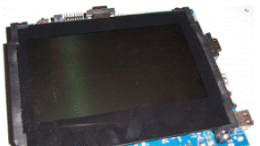
图3. 评估板EVAL-AD7768FMCZ外形图
责任编辑:HanFeng
【免责声明】
1、本文内容、数据、图表等来源于网络引用或其他公开资料,版权归属原作者、原发表出处。若版权所有方对本文的引用持有异议,请联系拍明芯城(marketing@iczoom.com),本方将及时处理。
2、本文的引用仅供读者交流学习使用,不涉及商业目的。
3、本文内容仅代表作者观点,拍明芯城不对内容的准确性、可靠性或完整性提供明示或暗示的保证。读者阅读本文后做出的决定或行为,是基于自主意愿和独立判断做出的,请读者明确相关结果。
4、如需转载本方拥有版权的文章,请联系拍明芯城(marketing@iczoom.com)注明“转载原因”。未经允许私自转载拍明芯城将保留追究其法律责任的权利。
拍明芯城拥有对此声明的最终解释权。


 产品分类
产品分类




 2012- 2022 拍明芯城ICZOOM.com 版权所有 客服热线:400-693-8369 (9:00-18:00)


