


 产品分类
产品分类
基于Altera公司的Cyclone V SoC FPGA 系列开发方案
 258
258
 拍明
拍明
原标题:Altera Cyclone V SoC FPGA 系列开发方案
Altera公司的Cyclone V SoC FPGA 系列基于28nm低功耗(LP)工艺,提供需要5G收发器应用的最低功耗,和以前的产品检验相比,功耗降低40%.器件集成了基于ARM处理器的硬件处理器系统(HPS),具有更有效的逻辑综合功能,收发器系列和SoC FPGA系列,从而降低系统功耗,成本和产品上市时间,主要用在工业,无线和有线通信,军用设备和汽车市场.本文介绍了Cyclone V SoC FPGA 系列主要优势和特性,架构图,HPS特性以及Cyclone V SX SoC开发板主要特性,框图和电路图.
Altera’s Cyclone® V FPGAs provide the industry’s lowest system cost and power, along with performance levels that make the device family ideal for differentiating your high-volume applications. You’ll get up to 40 percent lower total power compared with the previous generation, efficient logic integration capabilities, integrated transceiver variants, and SoC FPGA variants with an ARM®-based hard processor system (HPS).
The Cyclone® V devices are designed to simultaneously accommodate the shrinking power consumption, cost, and time-to-market requirements; and the increasing bandwidth requirements for high-volume and cost-sensitive applications.
Enhanced with integrated transceivers and hard memory controllers, the Cyclone® V devices are suitable for applications in the industrial, wireless and wireline, military, and automotive markets.
Built on the 28-nm low power (LP) process technology, Altera’s Cyclone V FPGAs deliver the lowest power solution for applications requiring up to 5G transceivers. Compared to previous generations, Cyclone V FPGAs offer a 40-percent power reduction, with a balance of power reduction from all areas.

图1.Cyclone V SoC FPGA架构图

图2.Cyclone V SoC框图
硬件处理器系统(HPS)特性:
925 MHz, dual-core ARM® Cortex™-A9 MPCore™ processor
Each processor core includes:
32 KB of L1 instruction cache, 32 KB of L1 data cache
Single- and double-precision floating-point unit and NEONTM media engine
CoreSightTM debug and trace technology
512 KB of shared L2 cache
64 KB of scratch RAM
Multiport SDRAM controller with support for DDR2, DDR3, and LPDDR2 and optional error correction code (ECC) support
8-channel direct memory access (DMA) controller
QSPI flash controller
NAND flash controller with DMA
SD/SDIO/MMC controller with DMA
2x 10/100/1000 Ethernet media access control (MAC) with DMA
2x USB On-The-Go (OTG) controller with DMA
4x I2C controller
2x UART
2x serial peripheral interface (SPI) master peripherals, 2x SPI slave peripherals
Up to 134 general-purpose I/O (GPIO)
7x general-purpose timers
4x watchdog timers
High-Bandwidth HPS-to-FPGA Interconnect Backbone
Although the HPS and the FPGA can operate independently, they are tightly coupled via a high-bandwidth system interconnect built from high-performance ARM AMBA® AXITM bus bridges. IP bus masters in the FPGA fabric have access to HPS bus slaves via the FPGA-to-HPS interconnect. Similarly, HPS bus masters have access to bus slaves in the FPGA fabric via the HPS-to-FPGA bridge. Both bridges are AMBA AXI-3 compliant and support simultaneous read and write transactions. Up to six FPGA masters can share the HPS SDRAM controller with the processor. Additionally, the processor can be used to configure the FPGA fabric under program control via a dedicated 32 bit configuration port.
HPS-to-FPGA: configurable 32, 64, or 128 bit AMBA AXI interface
FPGA-to-HPS: configurable 32, 64, or 128 bit AMBA AXI interface
FPGA-to-HPS SDRAM controller: up to 6 masters (command ports), 4x 64 bit read data ports and 4x 64 bit write data ports
32 bit FPGA configuration manager
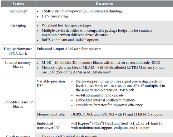
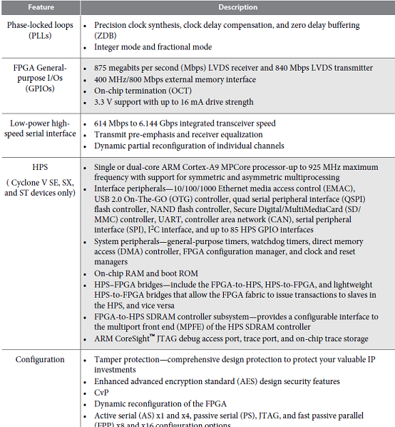
Cyclone V 系列产品主要优势:


Cyclone V 系列产品主要特性:
Cyclone V SX SoC开发板
The Altera® Cyclone® V SoC Development Kit offers a quick and simple approach to develop custom ARM® processor-based SoC designs accompanied by Altera’s low-power, low-cost Cyclone V FPGA fabric.
Cyclone V SX SoC开发板主要特性:
Processor and FPGA prototyping and power measurement
Industrial networking protocols
Motor control applications*
Acceleration of image- and video-processing applications*
PCI Express® (PCIe®) x4 lane with ~1,000 MBps transfer rate (endpoint or rootport)
*Application-specific daughtercards, available separately, supporting a wide range of I/O and interface standards.
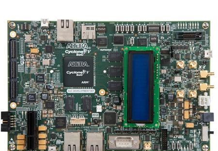
图3. Cyclone V SX SoC开发板外形图
Cyclone V SX SoC开发板包含:
Cyclone V SX development board
Featured devices
Cyclone V SX SoC—5CSXFC6D6F31C6N (SoC)
MAX® V CPLD—5M2210ZF256C4N (system controller)
MAX II CPLD—EPM570GF100 (embedded USB-BlasterTM II cable)
FPGA configuration sources
Embedded USB-Blaster II (JTAG) cable
EPCQ flash (PFL)
Hard processor system (HPS)
FPGA memory
1 GB DDR3 SDRAM (32 bit)
FPGA I/O interfaces
2X 10/100 Megabit Ethernet PHYs (EtherCAT)
PCIe Gen1 x4 female connector
Universal high-speed mezzanine card (HSMC)—x4 transceivers, x16 TX LVDS, x16 RX LVDS
One serial digital interface (SDI) channel
Four SMAs for one transceiver channel
4X push buttons
2X switches
4X LEDs
HPS boot sources
128 MB quad serial peripheral interface (SPI) flash memory
Removable micro-SD card flash memory
FPGA
HPS memory
1 GB DDR3 SDRAM (32 bit) with error correction code (ECC)
128 MB quad SPI flash memory
Micro-SD card socket with 4 GB micro-SD card flash device
HPS I/O interfaces
1X USB 2.0 On-the-Go (OTG)
1X 10/100/1000 Megabit Ethernet (10MbE/100MbE/1000MbE)
1X CAN
1X UART (UART to USB bridge)
1X real-time clock (with battery backup)
1X two-line text LCD
1-/2-channel, 20 bit delta-sigma analog-to-digital converter (Linear Technology LTC2422)
4X push buttons
4X switches
4X LEDs
Clocking
Four-output programmable clock generator for FPGA reference clock inputs
125 MHz LVDS oscillator for FPGA reference clock input
148.5 MHz LVDS programmable voltage-controlled crystal oscillator (VCXO) for FPGA reference clock input
50 MHz single-ended oscillator for FPGA and MAX V FPGA clock input
100 MHz single-ended oscillator for MAX V FPGA configuration clock input
SMA input for HPS clock
Power
Laptop DC input 14—20 V adapter
System monitoring circuit
Power (voltage, current, wattage)
HSMC breakout board
HSMC loopback board
Mechanical
Board dimensions—8.19” x 5.22”
Cyclone V SX FPGA Development Kit software content (downloadable from Table 2)
Design examples
Board test system (BTS)*
Golden System Reference Design with Board Update Portal web server
Complete documentation (see Table 2)
SoC Embedded Design Suite Standard Edition
ARM Development Studio 5 (DS-5™) Altera Edition Toolkit
Hardware-to-software handoff tools
Linux run-time software for application development
SoC hardware libraries for firmware development
Application examples
Free software supported by Quartus® Prime Lite and Standard Edition software

图4. Cyclone V SX SoC开发板框图
责任编辑:HanFeng
【免责声明】
1、本文内容、数据、图表等来源于网络引用或其他公开资料,版权归属原作者、原发表出处。若版权所有方对本文的引用持有异议,请联系拍明芯城(marketing@iczoom.com),本方将及时处理。
2、本文的引用仅供读者交流学习使用,不涉及商业目的。
3、本文内容仅代表作者观点,拍明芯城不对内容的准确性、可靠性或完整性提供明示或暗示的保证。读者阅读本文后做出的决定或行为,是基于自主意愿和独立判断做出的,请读者明确相关结果。
4、如需转载本方拥有版权的文章,请联系拍明芯城(marketing@iczoom.com)注明“转载原因”。未经允许私自转载拍明芯城将保留追究其法律责任的权利。
拍明芯城拥有对此声明的最终解释权。
相关资讯
:
基于MC33771主控芯片的新能源锂电池管理系统解决方案

AMIC110 32位Sitara ARM MCU开发方案

基于AMIC110多协议可编程工业通信处理器的32位Sitara ARM MCU开发方案

基于展讯SC9820超低成本LTE芯片平台的儿童智能手表解决方案

基于TI公司的AM437x双照相机参考设计

基于MTK6580芯片的W2智能手表解决方案


 2012- 2022 拍明芯城ICZOOM.com 版权所有 客服热线:400-693-8369 (9:00-18:00)


