


 产品分类
产品分类
基于NXP公司的KW40Z低功耗蓝牙(BLE)心率监测仪参考设计
 239
239
 拍明
拍明
原标题:NXPKW40Z低功耗蓝牙(BLE)心率监测仪参考设计
NXP公司的KW40Z/30Z/20Z是超低功耗高度集成系统级芯品(SoC),集成了工作频率2.36 GHz到2.48 GHz的无线收发器,支持FSK/GFSK和O-QPSK调制器;以及ARM Cortex-M0+CPU, 160 KB闪存和20KB SRAM,BLE链接层硬件,802.15.4包处理器硬件和外设,支持蓝牙低功耗(BLE)或IEEE标准802.15.4 RF连接,主要用在手持保健设备,可穿戴运动和健美设备,AV遥控,计算机键盘和鼠标,游戏控制器,接图控制,安全系统,智能能源和家庭局域网.本文介绍了KW40Z主要特性,框图,以及低功耗蓝牙(BLE)心率监测仪参考设计主要特性,框图,应用框图,软件架构图和电路图.
The KW40Z/30Z/20Z (called KW40Z throughout this document) is an ultra low-power,highly integrated single-chip device that enables Bluetooth low energy (BLE) or IEEE Standard 802.15.4 RF connectivity for portable, extremely low-power embeddedsystems. Applications include portable health care devices, wearable sports and fitnessdevices, AV remote controls, computer keyboards and mice, gaming controllers, accesscontrol, security systems, smart energy and home area networks.
The KW40Z SoC integrates a radio transceiver operating in the 2.36 GHz to 2.48 GHz range supporting a range of FSK/GFSK and O-QPSK modulations, an ARM Cortex-M0+CPU, 160 KB Flash and 20 KB SRAM, BLE Link Layer hardware, 802.15.4 packet processor hardware and peripherals optimized to meet the requirements of the target applications.
The KW40Z SoC’s radio frequency transceiver is compliant with Bluetooth version 4.1 for Low Energy (aka Bluetooth Smart), and the IEEE standard 802.15.4-2011 using OQPSKin the 2.4 GHz ISM band.
The KW40Z SoC can be used in applications as a "BlackBox" modem by simply adding BLE or IEEE Std. 802.15.4 connectivity to an existing embedded controller system, or used as a stand-alone smart wireless sensor with embedded application where no host controller is required.
Freescale provides fully certified protocol stacks and application profiles to supportKW40Z. The KW40Z Flash and SRAM memory are available for applications and communication protocols using a choice of Freescale or 3rd party software development tools.
The RF section of the KW40Z SoC is optimized to require very few externalcomponents, achieving the smallest RF footprint possible on a printed circuit board. Extremely long battery life is achieved though efficiency of code execution in the Cortex-M0+ CPU core and the multiple low power operating modes of the KW40Z SoC. Additionally, an integrated DC-DC converter enables a wide operating range from 0.9 V to 4.2 V. The DC-DC in Buck mode enables KW40Z to operate from a single coin cell battery with a significant reduction of peak Rx and Tx current consumption. The DC-DC in boost mode enables a single alkaline battery to be used throughout its entire useful voltage range of 0.9 V to 1.795 V.
KW40Z主要特性:
• Multi-Standard Radio
– 2.4 GHz Bluetooth Low Energy version 4.1compliant
– IEEE Standard 802.15.4 2011 compliant
– Typical Receiver Sensitivity (BLE) = -91 dBm
– Typical Receiver Sensitivity (802.15.4) = -102 dBm
– Programmable Transmitter Output Power: -18 dBmto +5 dBm
– Low external component counts for low costapplication
• MCU and Memories
– Up to 48 MHz ARM® Cortex-M0+ core
– On-chip 160 KB Flash memory
– On-chip 20 KB SRAM
• Low Power Consumption
– Typical Rx Current: 6.5 mA (DCDC in buck mode,3.6 V supply)
– Typical Tx Current: 8.4 mA (DCDC in buck mode,3.6 V supply) for a 0 dBm output
– Low Power Mode (VLLS0) Current: 206 nA
• Clocks
– 32 MHz Crystal Oscillator
– 32 kHz Crystal Oscillator
• System peripherals
– Nine low-power modes to provide poweroptimization based on application requirements
– DCDC Converter supporting Buck, Boost, and
Bypass modes
– DMA Controller
– COP Software watchdog
– SWD Interface and Micro Trace buffer
– Bit Manipulation Engine (BME)
• Human-machine interface
– Touch Sensing Input
– General-purpose input/output
• Analog modules
– 16-bit Analog-to-Digital Converter (ADC)
– 12-bit Digital-to-Analog Converter (DAC)
– 6-bit High Speed Analog Comparator (CMP)
• Timers
– 16-bit low-power timer (LPTMR)
– 3 Timers Modules(TPM): One 4 channels TPM andTwo 2 channels TPMs
– Programmable Interrupt Timer (PIT)
– Real-Time Clock (RTC)
• Communication interfaces
– 2 SPI modules
– 2 I2C modules
– Low Power UART module
– Carrier Modulator Timer (CMT)
• Security
– AES-128 Accelerator (AESA)
– True Random Number Generator (TRNG)
• Operating Characteristics
– DCDC Converter supporting Buck, Boost, andBypass modes
– Temperature range (ambient): -40 to 85°C
Radio features
Operating frequencies:
• 2.4 GHz ISM band (2400-2483.5 MHz)
• MBAN 2360-2400 MHz
Supported standards:
• Bluetooth v4.1 Low Energy compliant 1 Mbps GFSK modulation
• IEEE Std. 802.15.4-2011 compliant O-QPSK modulation
• Freescale Thread Networking Stack
• Bluetooth Low Energy(BLE) Application Profiles
• ZigBee PRO and application profiles
Receiver performance:
• Receive sensitivity of -91 dBm for BLE
• Receive sensitivity of -102 dBm typical for IEEE Std. 802.15.4
Other features:
• Programmable transmit output power from -18 dBm to +5 dBm with DC/DC bypassand buck modes of operation
• Bluetooth Low Energy Link Layer hardware
• Hardware acceleration for IEEE Std. 802.15.4 packet processing
• 32 MHz crystal reference oscillator
• Supports antenna diversity option for IEEE Std. 802.15.4
• Supports dual PAN for IEEE Std. 802.15.4 with hardware-assisted address matchingacceleration
• Differential RF port shared by transmit and receive
• Low external component count
• Supports transceiver range extension using external PA and/or LNA
Microcontroller features
ARM Cortex-M0+ CPU
• Up to 48 MHz CPU
• As compared to Cortex-M0, the Cortex-M0+ uses an optimized 2-stage pipeline
microarchitecture for reduced power consumption and improved architectural
performance (cycles per instruction)
• Supports up to 32 interrupt request sources
• Binary compatible instruction set architecture with the Cortex-M0 core
• Thumb instruction set combines high code density with 32-bit performance
• Serial Wire Debug (SWD) reduces the number of pins required for debugging
• Micro Trace Buffer (MTB) provides lightweight program trace capabilities usingsystem RAM as the destination memory
Nested Vectored Interrupt Controller (NVIC)
• 32 vectored interrupts, 4 programmable priority levels
• Includes a single non-maskable interrupt
Wake-up Interrupt Controller (WIC)
• Supports interrupt handling when system clocking is disabled in low power modes
• Takes over and emulates the NVIC behavior when correctly primed by the NVIC on
entry to very-deep-sleep
• A rudimentary interrupt masking system with no prioritization logic signals forwake-up as soon as a non-masked interrupt is detected
Debug Controller
• Two-wire Serial Wire Debug (SWD) interface
• Hardware breakpoint unit for 2 code addresses
• Hardware watchpoint unit for 2 data items
• Micro Trace Buffer for program tracing
On-Chip Memory
• 160 KB Flash
• Firmware distribution protection. Flash can be marked execute-only on a persector
(4 KB) basis to prevent firmware contents from being read by 3rd parties
• Flash implemented as one 128 KB block and one 32 KB block. Code canexecute or read from one block while the other block is being erased orprogrammed
• 20 KB SRAM
• Security circuitry to prevent unauthorized access to RAM and flash contents through
the debugger
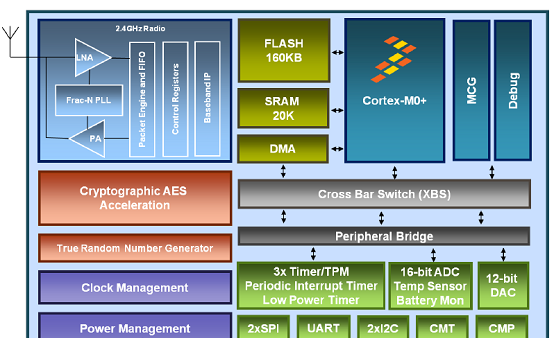
图1.KW40Z/KW30Z/KW20Z简化框图
低功耗蓝牙(BLE)心率监测仪参考设计
The BLE Heart Rate Monitor reference design demonstrates the implementation of a wireless electrocardiogram (ECG) acquisition system. It features the Freescale MKW40 system on chip (SoC) which includes an ARM® CortexTM M0+ processor together with a 2.4 GHz radio for BLE and 802.15.4.
The ECG signal is obtained from the finger tips and processed by the MKW40 SoC. Bluetooth® Low Energy (BLE)心率监测仪参考设计演示了无线心电图(ECG)采集系统是如何实现的。它采用KW40Z片上系统(SOC)。该系统包括一个ARM® Cortex® M0+处理器,并配备了面向BLE和802.15.4的2.4 GHz无线电。
ECG信号从指尖采集,并通过Kinetis KW40Z SoC处理。然后,计算用户的心率,并通过BLE传输给智能手机应用。该参考设计可由锂离子纽扣电池供电。由于Kinetis KW40Z MCU的低功耗特性,一个3.6V 200mA/h锂离子可充电纽扣电池可在连续使用的情况下供电长达40小时。恩智浦MC34671用作该器件的电池充电器解决方案。
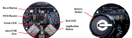
图2.低功耗蓝牙(BLE)心率监测仪参考设计外形图
低功耗蓝牙(BLE)心率监测仪参考设计主要特性:
包括恩智浦超低功耗的Kinetis KW40Z SoC BLE/ZigBee平台。由于该解决方案的低功耗特性,只需采用一个小小的纽扣电池就能连续运行40小时。
完全符合Bluetooth v4.1 Low Energy
差分输入/输出端口与外部混频变压器结合使用,实现单端口操作
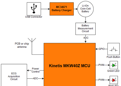
图3.低功耗蓝牙(BLE)心率监测仪参考设计框图
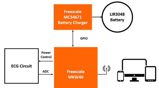
图4.低功耗蓝牙(BLE)心率监测仪参考设计应用框图

图5.低功耗蓝牙(BLE)心率监测仪参考设计软件架构图
责任编辑:HanFeng
【免责声明】
1、本文内容、数据、图表等来源于网络引用或其他公开资料,版权归属原作者、原发表出处。若版权所有方对本文的引用持有异议,请联系拍明芯城(marketing@iczoom.com),本方将及时处理。
2、本文的引用仅供读者交流学习使用,不涉及商业目的。
3、本文内容仅代表作者观点,拍明芯城不对内容的准确性、可靠性或完整性提供明示或暗示的保证。读者阅读本文后做出的决定或行为,是基于自主意愿和独立判断做出的,请读者明确相关结果。
4、如需转载本方拥有版权的文章,请联系拍明芯城(marketing@iczoom.com)注明“转载原因”。未经允许私自转载拍明芯城将保留追究其法律责任的权利。
拍明芯城拥有对此声明的最终解释权。
相关资讯
:
基于MC33771主控芯片的新能源锂电池管理系统解决方案

AMIC110 32位Sitara ARM MCU开发方案

基于AMIC110多协议可编程工业通信处理器的32位Sitara ARM MCU开发方案

基于展讯SC9820超低成本LTE芯片平台的儿童智能手表解决方案

基于TI公司的AM437x双照相机参考设计

基于MTK6580芯片的W2智能手表解决方案


 2012- 2022 拍明芯城ICZOOM.com 版权所有 客服热线:400-693-8369 (9:00-18:00)


